SNAS660D June   2015  – May 2021 LM53600-Q1 , LM53601-Q1

PRODUCTION DATA  

  1. Features
  2. Applications
  3. Description
  4. Revision History
  5. Device Comparison
  6. Pin Configuration and Functions
  7. Specifications
    1. 7.1 Absolute Maximum Ratings
    2. 7.2 ESD Ratings
    3. 7.3 Recommended Operating Conditions
    4. 7.4 Thermal Information
    5. 7.5 Electrical Characteristics
    6. 7.6 System Characteristics
    7. 7.7 Timing Requirements
    8. 7.8 Typical Characteristics
  8. Detailed Description
    1. 8.1 Overview
    2. 8.2 Functional Block Diagram
    3. 8.3 Feature Description
      1. 8.3.1 Control Scheme
      2. 8.3.2 Soft-Start Function
      3. 8.3.3 Current Limit
      4. 8.3.4 Hiccup Mode
      5. 8.3.5 RESET Function
      6. 8.3.6 Forced PWM Operation
      7. 8.3.7 Auto Mode Operation and IQ_VIN
      8. 8.3.8 SYNC Operation
      9. 8.3.9 Spread Spectrum
    4. 8.4 Device Functional Modes
      1. 8.4.1 Shutdown
      2. 8.4.2 FPWM Operation
      3. 8.4.3 Auto Mode Operation
  9. Applications and Implementation
    1. 9.1 Application Information
    2. 9.2 Typical Applications
      1. 9.2.1 Off-Battery 5-V, 1-A Output Automotive Converter with Spread Spectrum
        1. 9.2.1.1 Design Requirements
        2. 9.2.1.2 Detailed Design Procedure
          1. 9.2.1.2.1 Inductor Selection
          2. 9.2.1.2.2 Output Capacitor Selection
          3. 9.2.1.2.3 Input Capacitor Selection
          4. 9.2.1.2.4 FB Voltage Divider for Adjustable Versions
          5. 9.2.1.2.5 RPU - RESET Pull Up Resistor
        3. 9.2.1.3 Application Curves
      2. 9.2.2 Off-Battery 3.3 V, 1 A Output Automotive Converter with Spread Spectrum
        1. 9.2.2.1 Design Requirements
        2. 9.2.2.2 Design Procedure
        3. 9.2.2.3 Application Curves
    3. 9.3 Do's and Don't's
  10. 10Power Supply Recommendations
  11. 11Layout
    1. 11.1 Layout Guidelines
      1. 11.1.1 Ground and Thermal Plane Considerations
    2. 11.2 Layout Example
  12. 12Device and Documentation Support
    1. 12.1 Documentation Support
      1. 12.1.1 Related Documentation
    2. 12.2 Receiving Notification of Documentation Updates
    3. 12.3 Support Resources
    4. 12.4 Trademarks
    5. 12.5 Electrostatic Discharge Caution
    6. 12.6 Glossary
  13. 13Mechanical, Packaging, and Orderable Information

Typical Characteristics

VIN = 13.5 V, TA = 25°C (unless otherwise noted). Specified temperatures are ambient.
GUID-8AB8C279-6D65-465F-8B36-6A856431E813-low.gif
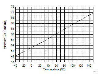
Device Type = 3.3-V Fixed Output
Input Voltage = 20 V Load = 500 mA
Figure 7-1 Minimum On-Time vs Temperature
GUID-5138ED29-30B0-4DBD-BDBA-C1C51FEEB46F-low.gif
 
 
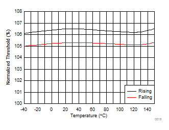
Figure 7-3 Upper RESET Threshold
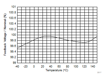
GUID-A166523B-4C2E-4724-8C4A-52455B37F02E-low.gifFigure 7-5 Normalized VFB vs Temperature
GUID-56DACC22-4AC4-401F-A370-E44F1FEE467B-low.gif
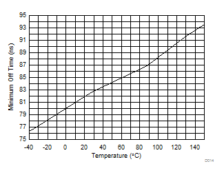
Device Type = 1 A 5-V Fixed Output In Dropout
Output = 4.85 V Load = 500 mA
Figure 7-2 Minimum Off-Time vs Temperature
GUID-F2AEB818-2CD9-423E-A876-B314E26917DD-low.gif
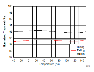
Margin is the difference between the falling RESET threshold and actual regulation voltage which includes the effects of temperature.
Figure 7-4 Lower Reset Threshold
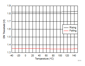
GUID-08D694A7-69A3-4238-B984-7A0EAC483868-low.gifFigure 7-6 EN Threshold vs Temperature