SNAS660D June   2015  – May 2021 LM53600-Q1 , LM53601-Q1

PRODUCTION DATA  

  1. Features
  2. Applications
  3. Description
  4. Revision History
  5. Device Comparison
  6. Pin Configuration and Functions
  7. Specifications
    1. 7.1 Absolute Maximum Ratings
    2. 7.2 ESD Ratings
    3. 7.3 Recommended Operating Conditions
    4. 7.4 Thermal Information
    5. 7.5 Electrical Characteristics
    6. 7.6 System Characteristics
    7. 7.7 Timing Requirements
    8. 7.8 Typical Characteristics
  8. Detailed Description
    1. 8.1 Overview
    2. 8.2 Functional Block Diagram
    3. 8.3 Feature Description
      1. 8.3.1 Control Scheme
      2. 8.3.2 Soft-Start Function
      3. 8.3.3 Current Limit
      4. 8.3.4 Hiccup Mode
      5. 8.3.5 RESET Function
      6. 8.3.6 Forced PWM Operation
      7. 8.3.7 Auto Mode Operation and IQ_VIN
      8. 8.3.8 SYNC Operation
      9. 8.3.9 Spread Spectrum
    4. 8.4 Device Functional Modes
      1. 8.4.1 Shutdown
      2. 8.4.2 FPWM Operation
      3. 8.4.3 Auto Mode Operation
  9. Applications and Implementation
    1. 9.1 Application Information
    2. 9.2 Typical Applications
      1. 9.2.1 Off-Battery 5-V, 1-A Output Automotive Converter with Spread Spectrum
        1. 9.2.1.1 Design Requirements
        2. 9.2.1.2 Detailed Design Procedure
          1. 9.2.1.2.1 Inductor Selection
          2. 9.2.1.2.2 Output Capacitor Selection
          3. 9.2.1.2.3 Input Capacitor Selection
          4. 9.2.1.2.4 FB Voltage Divider for Adjustable Versions
          5. 9.2.1.2.5 RPU - RESET Pull Up Resistor
        3. 9.2.1.3 Application Curves
      2. 9.2.2 Off-Battery 3.3 V, 1 A Output Automotive Converter with Spread Spectrum
        1. 9.2.2.1 Design Requirements
        2. 9.2.2.2 Design Procedure
        3. 9.2.2.3 Application Curves
    3. 9.3 Do's and Don't's
  10. 10Power Supply Recommendations
  11. 11Layout
    1. 11.1 Layout Guidelines
      1. 11.1.1 Ground and Thermal Plane Considerations
    2. 11.2 Layout Example
  12. 12Device and Documentation Support
    1. 12.1 Documentation Support
      1. 12.1.1 Related Documentation
    2. 12.2 Receiving Notification of Documentation Updates
    3. 12.3 Support Resources
    4. 12.4 Trademarks
    5. 12.5 Electrostatic Discharge Caution
    6. 12.6 Glossary
  13. 13Mechanical, Packaging, and Orderable Information

Layout Example

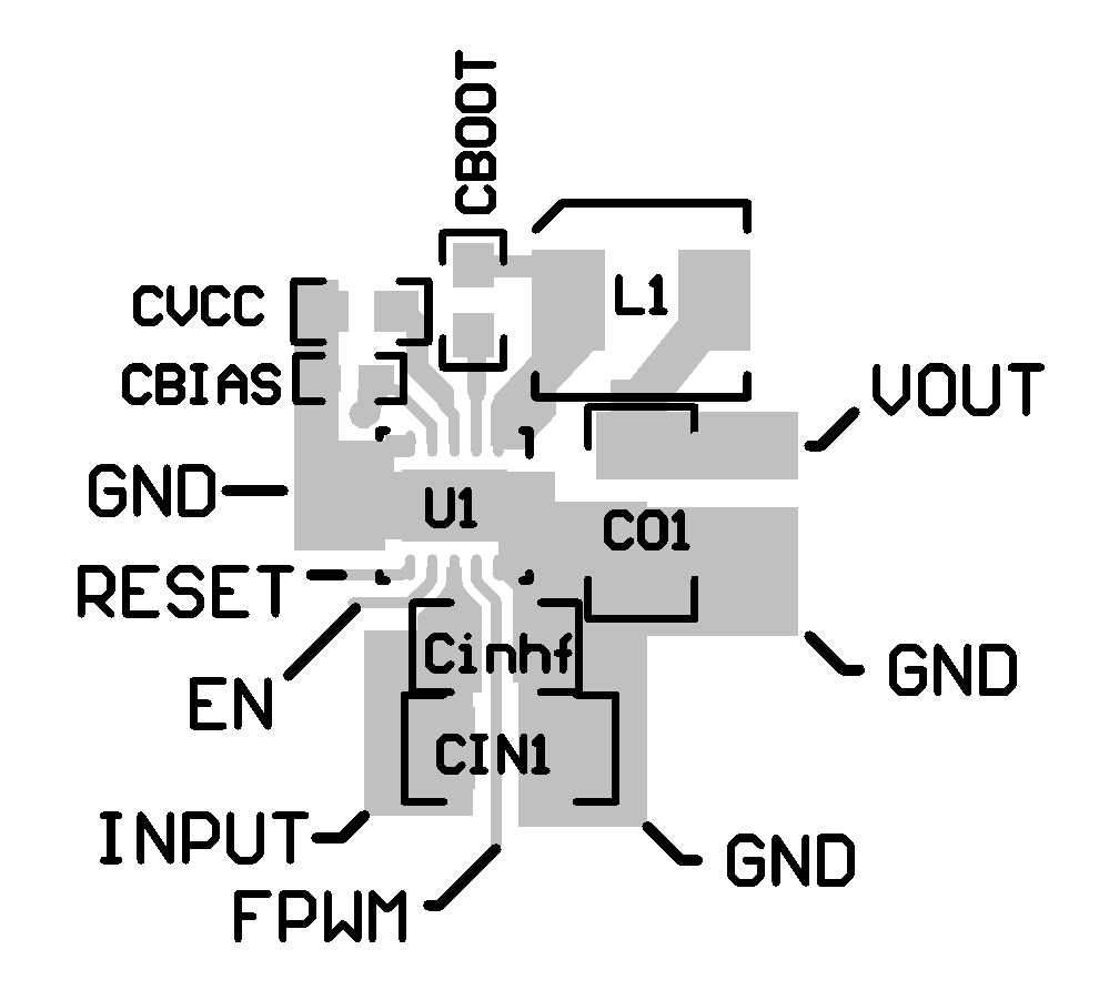
GUID-2CD8173B-1186-431B-8FE0-05F767CFE5C1-low.pngFigure 11-2 Fixed Output Version

Figure 11-2 shows an example layout for a fixed output version of the LM53600-Q1 and LM53601-Q1 similar to the one used in the Rev A EVM. Note that the via next to CBIAS connects on the back side of the board to VOUT near CO1. This layout shows 10 µF of output capacitance and 4.7 µF of input capacitance. An additional >10 µF of output capacitance and about 4.7 µF of input capacitance is assumed to be elsewhere in the system. A solid, unbroken ground plane is under this entire circuit except immediately below the SW node.