SNAS663B March 2017 – July 2019 LMK04616
PRODUCTION DATA.
3 Description
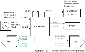
The LMK0461x device family is the industry’s highest performance and lowest power jitter cleaner with JESD204B support. The 16 clock outputs can be configured to drive eight JESD204B converters or other logic devices using device and SYSREF clocks. The 17th output can be configured to provide a signal from PLL2 or a copy from the external VCXO.
Features like fully integrated PLL1 and PLL2 loop filters, a high number of integrated LDOs, digital and analog delay, the flexibility to supply outputs with 3.3V, 2.5V and 1.8V as well as the option to generate multiple SYSREF domains simultaneously makes the device easy to use.
Not limited to JESD204B applications each of the 17 outputs can be configured for traditional clocking systems.
- For all available packages, see the orderable addendum at the end of the data sheet.
Simplified Schematic
