SNAS668E August 2015 – September 2024 LMK03328
PRODUCTION DATA
- 1
- 1 Features
- 2 Applications
- 3 Description
- 4 Device Comparison
- 5 Pin Configuration and Functions
-
6 Specifications
- 6.1 Absolute Maximum Ratings
- 6.2 ESD Ratings
- 6.3 Recommended Operating Conditions
- 6.4 Thermal Information
- 6.5 Thermal Information
- 6.6 Electrical Characteristics - Power Supply
- 6.7 Pullable Crystal Characteristics (SECREF_P, SECREF_N)
- 6.8 Non-Pullable Crystal Characteristics (SECREF_P, SECREF_N)
- 6.9 Clock Input Characteristics (PRIREF_P/PRIREF_N, SECREF_P/SECREF_N)
- 6.10 VCO Characteristics
- 6.11 PLL Characteristics
- 6.12 1.8-V LVCMOS Output Characteristics (OUT[7:0])
- 6.13 LVCMOS Output Characteristics (STATUS[1:0]
- 6.14 Open-Drain Output Characteristics (STATUS[1:0])
- 6.15 AC-LVPECL Output Characteristics
- 6.16 AC-LVDS Output Characteristics
- 6.17 AC-CML Output Characteristics
- 6.18 HCSL Output Characteristics
- 6.19 Power-On/Reset Characteristics
- 6.20 2-Level Logic Input Characteristics (HW_SW_CTRL, PDN, GPIO[5:0])
- 6.21 3-Level Logic Input Characteristics (REFSEL, GPIO[3:1])
- 6.22 Analog Input Characteristics (GPIO[5])
- 6.23 I2C-Compatible Interface Characteristics (SDA, SCL)
- 6.24 Typical 156.25-MHz, Closed-Loop Output Phase Noise Characteristics
- 6.25 Typical 161.1328125-MHz, Closed-Loop Output Phase Noise Characteristics
- 6.26 Closed-Loop Output Jitter Characteristics
- 6.27 PCIe Clock Output Jitter
- 6.28 Typical Power Supply Noise Rejection Characteristics
- 6.29 Typical Power Supply Noise Rejection Characteristics
- 6.30 Typical Closed-Loop Output Spur Characteristics
- 6.31 Typical Characteristics
- 7 Parameter Measurement Information
-
8 Detailed Description
- 8.1 Overview
- 8.2 Functional Block Diagram
- 8.3 Feature Description
- 8.4
Device Functional Modes
- 8.4.1 Smart Input MUX
- 8.4.2 Universal Input Buffer (PRI_REF, SEC_REF)
- 8.4.3 Crystal Input Interface (SEC_REF)
- 8.4.4 Reference Doubler
- 8.4.5 Reference (R) Divider
- 8.4.6 Input (M) Divider
- 8.4.7 Feedback (N) Divider
- 8.4.8 Phase Frequency Detector (PFD)
- 8.4.9 Charge Pump
- 8.4.10 Loop Filter
- 8.4.11 VCO Calibration
- 8.4.12 Fractional Circuitry
- 8.4.13 Post Divider
- 8.4.14 High-Speed Output MUX
- 8.4.15 High-Speed Output Divider
- 8.4.16 High-Speed Clock Outputs
- 8.4.17 Output Synchronization
- 8.4.18 Status Outputs
- 8.5 Programming
-
9 Register Maps
- 9.1
LMK03328
Registers
- 9.1.1 VNDRID_BY1 Register; R0
- 9.1.2 VNDRID_BY0 Register; R1
- 9.1.3 PRODID Register; R2
- 9.1.4 REVID Register; R3
- 9.1.5 PARTID Register; R4
- 9.1.6 PINMODE_SW Register; R8
- 9.1.7 PINMODE_HW Register; R9
- 9.1.8 TARGETADR Register; R10
- 9.1.9 EEREV Register; R11
- 9.1.10 DEV_CTL Register; R12
- 9.1.11 INT_LIVE Register; R13
- 9.1.12 INT_MASK Register; R14
- 9.1.13 INT_FLAG_POL Register; R15
- 9.1.14 INT_FLAG Register; R16
- 9.1.15 INTCTL Register; R17
- 9.1.16 OSCCTL2 Register; R18
- 9.1.17 STATCTL Register; R19
- 9.1.18 MUTELVL1 Register; R20
- 9.1.19 MUTELVL2 Register; R21
- 9.1.20 OUT_MUTE Register; R22
- 9.1.21 STATUS_MUTE Register; R23
- 9.1.22 DYN_DLY Register; R24
- 9.1.23 REFDETCTL Register; R25
- 9.1.24 STAT0_INT Register; R27
- 9.1.25 STAT1 Register; R28
- 9.1.26 OSCCTL1 Register; R29
- 9.1.27 PWDN Register; R30
- 9.1.28 OUTCTL_0 Register; R31
- 9.1.29 OUTCTL_1 Register; R32
- 9.1.30 OUTDIV_0_1 Register; R33
- 9.1.31 OUTCTL_2 Register; R34
- 9.1.32 OUTCTL_3 Register; R35
- 9.1.33 OUTDIV_2_3 Register; R36
- 9.1.34 OUTCTL_4 Register; R37
- 9.1.35 OUTDIV_4 Register; R38
- 9.1.36 OUTCTL_5 Register; R39
- 9.1.37 OUTDIV_5 Register; R40
- 9.1.38 OUTCTL_6 Register; R41
- 9.1.39 OUTDIV_6 Register; R42
- 9.1.40 OUTCTL_7 Register; R43
- 9.1.41 OUTDIV_7 Register; R44
- 9.1.42 CMOSDIVCTRL Register; R45
- 9.1.43 CMOSDIV0 Register; R46
- 9.1.44 CMOSDIV1 Register; R47
- 9.1.45 STATUS_SLEW Register; R49
- 9.1.46 IPCLKSEL Register; R50
- 9.1.47 IPCLKCTL Register; R51
- 9.1.48 PLL1_RDIV Register; R52
- 9.1.49 PLL1_MDIV Register; R53
- 9.1.50 PLL2_RDIV Register; R54
- 9.1.51 PLL2_MDIV Register; R55
- 9.1.52 PLL1_CTRL0 Register; R56
- 9.1.53 PLL1_CTRL1 Register; R57
- 9.1.54 PLL1_NDIV_BY1 Register; R58
- 9.1.55 PLL1_NDIV_BY0 Register; R59
- 9.1.56 PLL1_FRACNUM_BY2 Register; R60
- 9.1.57 PLL1_FRACNUM_BY1 Register; R61
- 9.1.58 PLL1_FRACNUM_BY0 Register; R62
- 9.1.59 PLL_FRACDEN_BY2 Register; R63
- 9.1.60 PLL1_FRACDEN_BY1 Register; R64
- 9.1.61 PLL1_FRACDEN_BY0 Register; R65
- 9.1.62 PLL1_MASHCTRL Register; R66
- 9.1.63 PLL1_LF_R2 Register; R67
- 9.1.64 PLL1_LF_C1 Register; R68
- 9.1.65 PLL1_LF_R3 Register; R69
- 9.1.66 PLL1_LF_C3 Register; R70
- 9.1.67 PLL2_CTRL0 Register; R71
- 9.1.68 PLL2_CTRL1 Register; R72
- 9.1.69 PLL2_NDIV_BY1 Register; R73
- 9.1.70 PLL2_NDIV_BY0 Register; R74
- 9.1.71 PLL2_FRACNUM_BY2 Register; R75
- 9.1.72 PLL2_FRACNUM_BY1 Register; R76
- 9.1.73 PLL2_FRACNUM_BY0 Register; R77
- 9.1.74 PLL2_FRACDEN_BY2 Register; R78
- 9.1.75 PLL2_FRACDEN_BY1 Register; R79
- 9.1.76 PLL2_FRACDEN_BY0 Register; R80
- 9.1.77 PLL2_MASHCTRL Register; R81
- 9.1.78 PLL2_LF_R2 Register; R82
- 9.1.79 PLL2_LF_C1 Register; R83
- 9.1.80 PLL2_LF_R3 Register; R84
- 9.1.81 PLL2_LF_C3 Register; R85
- 9.1.82 XO_MARGINING Register; R86
- 9.1.83 XO_OFFSET_GPIO5_STEP_1_BY1 Register; R88
- 9.1.84 XO_OFFSET_GPIO5_STEP_1_BY0 Register; R89
- 9.1.85 XO_OFFSET_GPIO5_STEP_2_BY1 Register; R90
- 9.1.86 XO_OFFSET_GPIO5_STEP_2_BY0 Register; R91
- 9.1.87 XO_OFFSET_GPIO5_STEP_3_BY1 Register; R92
- 9.1.88 XO_OFFSET_GPIO5_STEP_3_BY0 Register; R93
- 9.1.89 XO_OFFSET_GPIO5_STEP_4_BY1 Register; R94
- 9.1.90 XO_OFFSET_GPIO5_STEP_4_BY0 Register; R95
- 9.1.91 XO_OFFSET_GPIO5_STEP_5_BY1 Register; R96
- 9.1.92 XO_OFFSET_GPIO5_STEP_5_BY0 Register; R97
- 9.1.93 XO_OFFSET_GPIO5_STEP_6_BY1 Register; R98
- 9.1.94 XO_OFFSET_GPIO5_STEP_6_BY0 Register; R99
- 9.1.95 XO_OFFSET_GPIO5_STEP_7_BY1 Register; R100
- 9.1.96 XO_OFFSET_GPIO5_STEP_7_BY0 Register; R101
- 9.1.97 XO_OFFSET_GPIO5_STEP_8_BY1 Register; R102
- 9.1.98 XO_OFFSET_GPIO5_STEP_8_BY0 Register; R103
- 9.1.99 XO_OFFSET_SW_BY1 Register; R104
- 9.1.100 XO_OFFSET_SW_BY0 Register; R105
- 9.1.101 PLL1_CTRL2 Register; R117
- 9.1.102 PLL1_CTRL3 Register; R118
- 9.1.103 PLL1_CALCTRL0 Register; R119
- 9.1.104 PLL1_CALCTRL1 Register; R120
- 9.1.105 PLL2_CTRL2 Register; R131
- 9.1.106 PLL2_CTRL3 Register; R132
- 9.1.107 PLL2_CALCTRL0 Register; R133
- 9.1.108 PLL2_CALCTRL1 Register; R134
- 9.1.109 NVMSCRC Register; R135
- 9.1.110 NVMCNT Register; R136
- 9.1.111 NVMCTL Register; R137
- 9.1.112 NVMLCRC Register; R138
- 9.1.113 MEMADR_BY1 Register; R139
- 9.1.114 MEMADR_BY0 Register; R140
- 9.1.115 NVMDAT Register; R141
- 9.1.116 RAMDAT Register; R142
- 9.1.117 ROMDAT Register; R143
- 9.1.118 NVMUNLK Register; R144
- 9.1.119 REGCOMMIT_PAGE Register; R145
- 9.1.120 POR_CTRL Register; R173
- 9.1.121 XOCAPCTRL_BY1 Register; R199
- 9.1.122 XOCAPCTRL_BY0 Register; R200
- 9.2 EEPROM Map
- 9.1
LMK03328
Registers
-
10Application and Implementation
- 10.1 Application Information
- 10.2 Typical Applications
- 10.3 Power Supply Recommendations
- 10.4 Layout
- 11Device and Documentation Support
- 12Revision History
- 13Mechanical, Packaging, and Orderable Information
8.4.16 High-Speed Clock Outputs
Each output can be configured as AC-LVPECL, AC-LVDS, AC-CML, HCSL, or LVCMOS by programming R31, R32, R34, R35, R37, R39, R41, and R43. Each output has the option to be muted or not, in case the source that sent the output becomes invalid, by programming R22. An invalid source can be either a primary or secondary reference that is no longer present, or a PLL that is unlocked. When outputs are to be muted, R20 and R21 must each be programmed to 0xFF. Outputs 0 and 1 share an output supply (VDDO_01), as well as outputs 2 and 3 (VDDO_23). Outputs 4, 5, 6, and 7 have individual output supplies (VDDO_4, VDDO_5, VDDO_6, VDDO_7). Each output supply can be independently set to 1.8 V, 2.5 V, or 3.3 V. When a particular output is desired to be disabled, the bits [5:0] in the corresponding output control register (R31, R32, R34, R35, R37, R39, R41, or R43) must be set to 0x00. If any of outputs 4, 5, 6, and 7 and the output dividers are disabled, the corresponding supplies can be connected to GND.
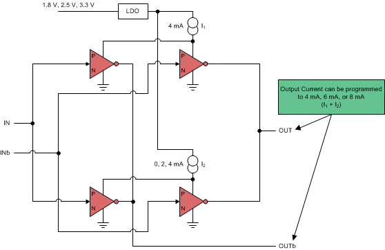
The AC-LVDS, AC-CML, and AC-LVPECL output structure is given in Figure 8-22 where the tail currents can be programmed to either 4 mA, 6 mA, or 8 mA to generate output voltage swings that are compatible with LVDS, CML, or LVPECL, respectively. Because this output structure is GND referenced, the output supplies can be operated from 1.8 V, 2.5 V, or 3.3 V, and offer lower power dissipation compared to traditional LVDS, CML, or LVPECL structures without any impact on jitter performance or other AC or DC specifications. Interfacing to LVDS, CML, or LVPECL receivers is accomplished using just an external AC-coupling capacitor for each output. No source termination is required, because the on-chip termination is automatically enabled when selecting AC-LVDS, AC-CML, or AC-LVPECL for good impedance matching to 50-Ω interconnects.
 Figure 8-22 Structure of AC-LVDS, AC-CML, and AC-LVPECL Output Stage
The HCSL output structure is open-drain and can be direct coupled or AC coupled to HCSL receivers with appropriate termination scheme. This output structure supports either on-chip 50-Ω termination or off-chip 50-Ω termination. The on-chip, 50-Ω termination is provided primarily for convenience when driving short traces. In the case of driving long traces possibly through a connector, the on-chip termination must be disabled and a 50 Ω to GND termination at the receiver must be implemented. The output supplies can be operated from 1.8 V, 2.5 V, or 3.3 V without any impact on jitter performance or other AC or DC specifications.
The LVCMOS outputs on each side (P and N) can be configured individually to be complementary or in-phase or can be turned off (high output impedance). The LVCMOS outputs are always at 1.8-V logic level irrespective of the output supply. In case 3.3-V LVCMOS outputs are required, STATUS1 and/or STATUS0 can be configured as 3.3-V LVCMOS outputs.
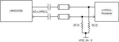
Figure 8-23 through Figure 8-28 show recommendations for interfacing between the LMK03328 high-speed clock outputs and LVCMOS, LVPECL, LVDS, CML, and HCSL receivers, respectively.
If 1.8-V LVCMOS signal from the high-speed clock outputs are desired to be interfaced with a 3.3-V LVCMOS receiver, a level shifter like LSF0101 must be used to convert the 1.8-V LVCMOS signal to a 3.3-V LVCMOS signal.
 Figure 8-23 Interfacing the LMK03328 1.8-V LVCMOS Output With 1.8-V LVCMOS Receiver
 Figure 8-24 Interfacing the LMK03328 1.8-V LVCMOS Output With 3.3-V LVCMOS Receiver
 Figure 8-25 Interfacing the LMK03328 AC-LVPECL Output With LVPECL Receiver
 Figure 8-26 Interfacing the LMK03328 AC-LVDS Output With LVDS Receiver
 Figure 8-27 Interfacing the LMK03328 AC-CML Output With CML Receiver
 Figure 8-28 Interfacing the LMK03328 Output With HCSL Receiver