SNAS674B September 2015 – February 2017 LMK61E2
PRODUCTION DATA.
- 1 Features
- 2 Applications
- 3 Description
- 4 Revision History
- 5 Pin Configuration and Functions
-
6 Specifications
- 6.1 Absolute Maximum Ratings
- 6.2 ESD Ratings
- 6.3 Recommended Operating Conditions
- 6.4 Thermal Information
- 6.5 Electrical Characteristics - Power Supply
- 6.6 LVPECL Output Characteristics
- 6.7 LVDS Output Characteristics
- 6.8 HCSL Output Characteristics
- 6.9 OE Input Characteristics
- 6.10 ADD Input Characteristics
- 6.11 Frequency Tolerance Characteristics
- 6.12 Power-On/Reset Characteristics (VDD)
- 6.13 I2C-Compatible Interface Characteristics (SDA, SCL)
- 6.14 PSRR Characteristics
- 6.15 Other Characteristics
- 6.16 PLL Clock Output Jitter Characteristics
- 6.17 Typical 156.25-MHz Output Phase Noise Characteristics
- 6.18 Typical 161.1328125 MHz Output Phase Noise Characteristics
- 6.19 Additional Reliability and Qualification
- 6.20 Typical Characteristics
- 7 Parameter Measurement Information
-
8 Detailed Description
- 8.1 Overview
- 8.2 Functional Block Diagram
- 8.3
Feature Description
- 8.3.1 Device Block-Level Description
- 8.3.2 Device Configuration Control
- 8.3.3 Register File Reference Convention
- 8.3.4 Configuring the PLL
- 8.3.5 Integrated Oscillator
- 8.3.6 Reference Doubler
- 8.3.7 Phase Frequency Detector
- 8.3.8 Feedback Divider (N)
- 8.3.9 Fractional Circuitry
- 8.3.10 Charge Pump
- 8.3.11 Loop Filter
- 8.3.12 VCO Calibration
- 8.3.13 High-Speed Output Divider
- 8.3.14 High-Speed Clock Output
- 8.3.15 Device Status
- 8.4 Device Functional Modes
- 8.5 Programming
- 8.6 EEPROM Map
- 8.7
Register Map
- 8.7.1
Register Descriptions
- 8.7.1.1 VNDRID_BY1 Register; R0
- 8.7.1.2 VNDRID_BY0 Register; R1
- 8.7.1.3 PRODID Register; R2
- 8.7.1.4 REVID Register; R3
- 8.7.1.5 SLAVEADR Register; R8
- 8.7.1.6 EEREV Register; R9
- 8.7.1.7 DEV_CTL Register; R10
- 8.7.1.8 XO_CAPCTRL_BY1 Register; R16
- 8.7.1.9 XO_CAPCTRL_BY0 Register; R17
- 8.7.1.10 DIFFCTL Register; R21
- 8.7.1.11 OUTDIV_BY1 Register; R22
- 8.7.1.12 OUTDIV_BY0 Register; R23
- 8.7.1.13 PLL_NDIV_BY1 Register; R25
- 8.7.1.14 PLL_NDIV_BY0 Register; R26
- 8.7.1.15 PLL_FRACNUM_BY2 Register; R27
- 8.7.1.16 PLL_FRACNUM_BY1 Register; R28
- 8.7.1.17 PLL_FRACNUM_BY0 Register; R29
- 8.7.1.18 PLL_FRACDEN_BY2 Register; R30
- 8.7.1.19 PLL_FRACDEN_BY1 Register; R31
- 8.7.1.20 PLL_FRACDEN_BY0 Register; R32
- 8.7.1.21 PLL_MASHCTRL Register; R33
- 8.7.1.22 PLL_CTRL0 Register; R34
- 8.7.1.23 PLL_CTRL1 Register; R35
- 8.7.1.24 PLL_LF_R2 Register; R36
- 8.7.1.25 PLL_LF_C1 Register; R37
- 8.7.1.26 PLL_LF_R3 Register; R38
- 8.7.1.27 PLL_LF_C3 Register; R39
- 8.7.1.28 PLL_CALCTRL Register; R42
- 8.7.1.29 NVMSCRC Register; R47
- 8.7.1.30 NVMCNT Register; R48
- 8.7.1.31 NVMCTL Register; R49
- 8.7.1.32 MEMADR Register; R51
- 8.7.1.33 NVMDAT Register; R52
- 8.7.1.34 RAMDAT Register; R53
- 8.7.1.35 NVMUNLK Register; R56
- 8.7.1.36 INT_LIVE Register; R66
- 8.7.1.37 SWRST Register; R72
- 8.7.1
Register Descriptions
-
9 Application and Implementation
- 9.1 Application Information
- 9.2
Typical Applications
- 9.2.1 Jitter Considerations in Serdes Systems
- 9.2.2 Frequency Margining
- 9.2.3 Design Requirements
- 10Power Supply Recommendations
- 11Layout
- 12Device and Documentation Support
- 13Mechanical, Packaging, and Orderable Information
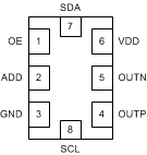
5 Pin Configuration and Functions
SIA Package
8-Pin QFM
Top View

Pin Functions
| PIN | I/O | DESCRIPTION | |
|---|---|---|---|
| NAME | NO. | ||
| POWER | |||
| GND | 3 | Ground | Device Ground. |
| VDD | 6 | Analog | 3.3-V Power Supply. |
| OUTPUT BLOCK | |||
| OUTP, OUTN | 4, 5 | Universal | Differential Output Pair (LVPECL, LVDS or HCSL). |
| DIGITAL CONTROL / INTERFACES | |||
| ADD | 2 | LVCMOS | When left open, LSB of I2C slave address is set to 01. When tied to VDD, LSB of I2C slave address is set to 10. When tied to GND, LSB of I2C slave address is set to 00. |
| OE | 1 | LVCMOS | Output Enable (internal pullup). When set to low, output pair is disabled and set at high impedance. |
| SCL | 8 | LVCMOS | I2C Serial Clock (open-drain). Requires an external pullup resistor to VDD. |
| SDA | 7 | LVCMOS | I2C Serial Data (bidirectional, open-drain). Requires an external pullup resistor to VDD. |