SNAS724A February 2018 – April 2018 LMK05028
PRODUCTION DATA.
- 1 Features
- 2 Applications
- 3 Description
- 4 Revision History
- 5 Description (continued)
- 6 Pin Configuration and Functions
- 7 Specifications
- 8 Parameter Measurement Information
-
9 Detailed Description
- 9.1 Overview
- 9.2 Functional Block Diagrams
- 9.3
Feature Description
- 9.3.1 Oscillator Input (XO_P/N)
- 9.3.2 TCXO/OCXO Input (TCXO_IN)
- 9.3.3 Reference Inputs (INx_P/N)
- 9.3.4 Clock Input Interfacing and Termination
- 9.3.5 Reference Input Mux Selection
- 9.3.6 Hitless Switching
- 9.3.7 Gapped Clock Support on Reference Inputs
- 9.3.8 Input Clock and PLL Monitoring, Status, and Interrupts
- 9.3.9
PLL Channels
- 9.3.9.1 PLL Frequency Relationships
- 9.3.9.2 Analog PLL (APLL)
- 9.3.9.3 APLL XO Doubler
- 9.3.9.4 APLL Phase Frequency Detector (PFD) and Charge Pump
- 9.3.9.5 APLL Loop Filter
- 9.3.9.6 APLL Voltage Controlled Oscillator (VCO)
- 9.3.9.7 APLL VCO Post-Dividers (P1, P2)
- 9.3.9.8 APLL Fractional N Divider (N) With SDM
- 9.3.9.9 REF-DPLL Reference Divider (R)
- 9.3.9.10 TCXO/OCXO Input Doubler and M Divider
- 9.3.9.11 TCXO Mux
- 9.3.9.12 REF-DPLL and TCXO-DPLL Time-to-Digital Converter (TDC)
- 9.3.9.13 REF-DPLL and TCXO-DPLL Loop Filter
- 9.3.9.14 REF-DPLL and TCXO-DPLL Feedback Dividers
- 9.3.10 Output Clock Distribution
- 9.3.11 Output Channel Muxes
- 9.3.12 Output Dividers
- 9.3.13 Clock Outputs (OUTx_P/N)
- 9.3.14 Glitchless Output Clock Start-Up
- 9.3.15 Clock Output Interfacing and Termination
- 9.3.16 Output Synchronization (SYNC)
- 9.3.17 Zero-Delay Mode (ZDM) Configuration
- 9.3.18 PLL Cascading With Internal VCO Loopback
- 9.4 Device Functional Modes
- 9.5 Programming
- 9.6 Register Maps
- 10Application and Implementation
- 11Power Supply Recommendations
- 12Layout
- 13Device and Documentation Support
- 14Mechanical, Packaging, and Orderable Information
9.2.2.1 PLL Output Clock Phase Noise Analysis in 3-Loop Mode
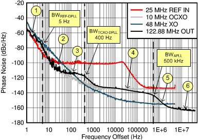
The following plot shows an example PLL clock output phase noise profile in 3-loop mode. The PLL output clock phase noise at different frequency offsets are determined by different noise contributors, such as external clock input sources (REF IN, OCXO, XO) and internal noise sources (PLL, VCO), as well as the configured PLL loop bandwidths (BWREF-DPLL, BWTCXO-DPLL, BWAPLL). The phase noise profile shown for each external clock source (fSOURCE) was normalized to the PLL output frequency (fOUT) by adding 20×LOG10(fOUT / fSOURCE) to the measured source's phase noise. The PLL output phase noise can be analyzed as follows:
- Below BWREF-DPLL, the REF input noise contributes to output.
- Above BWREF-DPLL, the REF input noise is attenuated by REF-DPLL bandwidth with up to 60-dB/decade roll-off.
- Below BWTCXO-DPLL, the OCXO noise and TDC noise of the TCXO-DPLL determine the output noise here. The close-in phase noise is –112 dBc/Hz at 100-Hz offset.
- Above BWTCXO-DPLL, the OCXO noise is attenuated. Below BWAPLL, the APLL noise dominates as the XO noise contribution is much lower.
- Above BWAPLL, the VCO noise dominates and the XO noise is attenuated.
- AC-LVPECL output noise floor is -163 dBc/Hz at 10-MHz offset.

| Output Phase Jitter = 160-fs RMS (12 kHz to 20 MHz) |
| AC-LVPECL output, fIN = 25 MHz, fTCXO = 10 MHz (OCXO), fXO = 48.0048 MHz, fTCXO-TDC = 20 MHz |