SNAS724A
February 2018 – April 2018
LMK05028
PRODUCTION DATA.
1
Features
2
Applications
3
Description
Device Images
Simplified Block Diagram
4
Revision History
5
Description (continued)
6
Pin Configuration and Functions
Pin Functions
6.1
Device Start-Up Modes
7
Specifications
7.1
Absolute Maximum Ratings
7.2
ESD Ratings
7.3
Recommended Operating Conditions
7.4
Thermal Information
7.5
Electrical Characteristics
7.6
Timing Diagrams
7.7
Typical Characteristics
8
Parameter Measurement Information
8.1
Output Clock Test Configurations
9
Detailed Description
9.1
Overview
9.1.1
ITU-T G.8262 (SyncE) Standards Compliance
9.2
Functional Block Diagrams
9.2.1
PLL Architecture Overview
9.2.2
3-Loop Mode
9.2.2.1
PLL Output Clock Phase Noise Analysis in 3-Loop Mode
9.2.3
2-Loop REF-DPLL Mode
9.2.4
2-Loop TCXO-DPLL Mode
9.2.5
PLL Configurations for Common Applications
9.3
Feature Description
9.3.1
Oscillator Input (XO_P/N)
9.3.2
TCXO/OCXO Input (TCXO_IN)
9.3.3
Reference Inputs (INx_P/N)
9.3.4
Clock Input Interfacing and Termination
9.3.5
Reference Input Mux Selection
9.3.5.1
Automatic Input Selection
9.3.5.2
Manual Input Selection
9.3.6
Hitless Switching
9.3.7
Gapped Clock Support on Reference Inputs
9.3.8
Input Clock and PLL Monitoring, Status, and Interrupts
9.3.8.1
XO Input Monitoring
9.3.8.2
TCXO Input Monitoring
9.3.8.3
Reference Input Monitoring
9.3.8.3.1
Reference Validation Timer
9.3.8.3.2
Amplitude Monitor
9.3.8.3.3
Missing Pulse Monitor (Late Detect)
9.3.8.3.4
Runt Pulse Monitor (Early Detect)
9.3.8.3.5
Frequency Monitoring
9.3.8.3.6
Phase Valid Monitor for 1-PPS Inputs
9.3.8.4
PLL Lock Detectors
9.3.8.5
Tuning Word History
9.3.8.6
Status Outputs
9.3.8.7
Interrupt
9.3.9
PLL Channels
9.3.9.1
PLL Frequency Relationships
9.3.9.2
Analog PLL (APLL)
9.3.9.3
APLL XO Doubler
9.3.9.4
APLL Phase Frequency Detector (PFD) and Charge Pump
9.3.9.5
APLL Loop Filter
9.3.9.6
APLL Voltage Controlled Oscillator (VCO)
9.3.9.6.1
VCO Calibration
9.3.9.7
APLL VCO Post-Dividers (P1, P2)
9.3.9.8
APLL Fractional N Divider (N) With SDM
9.3.9.9
REF-DPLL Reference Divider (R)
9.3.9.10
TCXO/OCXO Input Doubler and M Divider
9.3.9.11
TCXO Mux
9.3.9.12
REF-DPLL and TCXO-DPLL Time-to-Digital Converter (TDC)
9.3.9.13
REF-DPLL and TCXO-DPLL Loop Filter
9.3.9.14
REF-DPLL and TCXO-DPLL Feedback Dividers
9.3.10
Output Clock Distribution
9.3.11
Output Channel Muxes
9.3.11.1
TCXO/Ref Bypass Mux
9.3.12
Output Dividers
9.3.13
Clock Outputs (OUTx_P/N)
9.3.13.1
AC-Differential Output (AC-DIFF)
9.3.13.2
HCSL Output
9.3.13.3
LVCMOS Output (1.8 V, 2.5 V)
9.3.13.4
Output Auto-Mute During LOL or LOS
9.3.14
Glitchless Output Clock Start-Up
9.3.15
Clock Output Interfacing and Termination
9.3.16
Output Synchronization (SYNC)
9.3.17
Zero-Delay Mode (ZDM) Configuration
9.3.18
PLL Cascading With Internal VCO Loopback
9.4
Device Functional Modes
9.4.1
Device Start-Up Modes
9.4.1.1
EEPROM Mode
9.4.1.2
ROM Mode
9.4.2
PLL Operating Modes
9.4.2.1
Free-Run Mode
9.4.2.2
Lock Acquisition
9.4.2.3
Locked Mode
9.4.2.4
Holdover Mode
9.4.3
PLL Start-Up Sequence
9.4.4
Digitally-Controlled Oscillator (DCO) Mode
9.4.4.1
DCO Frequency Step Size
9.4.4.2
DCO Direct-Write Mode
9.4.5
Zero-Delay Mode (ZDM)
9.4.6
Cascaded PLL Operation
9.5
Programming
9.5.1
Interface and Control
9.5.2
I2C Serial Interface
9.5.2.1
I2C Block Register Transfers
9.5.3
SPI Serial Interface
9.5.3.1
SPI Block Register Transfer
9.5.4
Register Map Generation
9.5.5
General Register Programming Sequence
9.5.6
EEPROM Programming Flow
9.5.6.1
EEPROM Programming Using Register Commit (Method #1)
9.5.6.1.1
Write SRAM Using Register Commit
9.5.6.1.2
Program EEPROM
9.5.6.2
EEPROM Programming Using Direct SRAM Writes (Method #2)
9.5.6.2.1
Write SRAM Using Direct Writes
9.5.7
Read SRAM
9.5.8
Read EEPROM
9.5.9
EEPROM Start-Up Mode Default Configuration
9.6
Register Maps
10
Application and Implementation
10.1
Application Information
10.1.1
Device Start-Up Sequence
10.1.2
Power Down (PDN) Pin
10.1.3
Power Rail Sequencing, Power Supply Ramp Rate, and Mixing Supply Domains
10.1.3.1
Mixing Supplies
10.1.3.2
Power-On Reset (POR) Circuit
10.1.3.3
Powering Up From a Single-Supply Rail
10.1.3.4
Power Up From Split-Supply Rails
10.1.3.5
Non-Monotonic or Slow Power-Up Supply Ramp
10.1.4
Slow or Delayed XO Start-Up
10.2
Typical Application
10.2.1
Design Requirements
10.2.2
Detailed Design Procedure
10.2.3
Application Curves
10.3
Do's and Don'ts
11
Power Supply Recommendations
11.1
Power Supply Bypassing
12
Layout
12.1
Layout Guidelines
12.2
Layout Example
12.3
Thermal Reliability
13
Device and Documentation Support
13.1
Device Support
13.1.1
Clock Architect
13.1.2
TICS Pro
13.2
Documentation Support
13.2.1
Related Documentation
13.3
Receiving Notification of Documentation Updates
13.4
Community Resources
13.5
Trademarks
13.6
Electrostatic Discharge Caution
13.7
Glossary
14
Mechanical, Packaging, and Orderable Information
7.6
Timing Diagrams
Figure 2.
SPI Timing Parameters
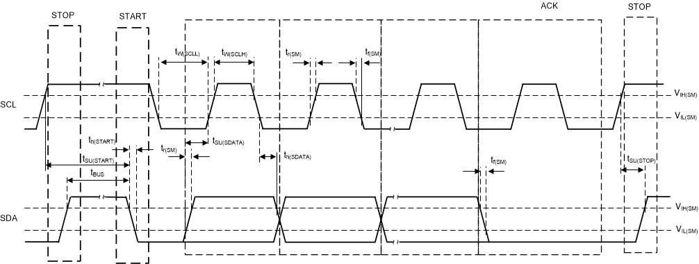
Figure 3.
I
2
C Timing Diagram
Figure 4.
Differential Output Voltage and Rise/Fall Time
Figure 5.
Single-Ended Output Voltage and Rise/Fall Time
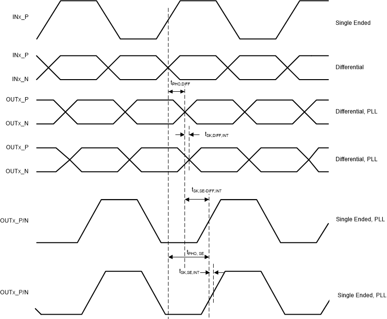
Figure 6.
Differential and Single-Ended Output Skew and Phase Offset