SNAS736C June   2017  – April 2019 LMX2595

PRODUCTION DATA.  

  1. Features
  2. Applications
  3. Description
    1.     Device Images
      1.      Simplified Schematic
  4. Revision History
  5. Pin Configuration and Functions
    1.     Pin Functions
  6. Specifications
    1. 6.1 Absolute Maximum Ratings
    2. 6.2 ESD Ratings
    3. 6.3 Recommended Operating Conditions
    4. 6.4 Thermal Information
    5. 6.5 Electrical Characteristics
    6. 6.6 Timing Requirements
    7. 6.7 Typical Characteristics
  7. Detailed Description
    1. 7.1 Overview
    2. 7.2 Functional Block Diagram
    3. 7.3 Feature Description
      1. 7.3.1  Reference Oscillator Input
      2. 7.3.2  Reference Path
        1. 7.3.2.1 OSCin Doubler (OSC_2X)
        2. 7.3.2.2 Pre-R Divider (PLL_R_PRE)
        3. 7.3.2.3 Programmable Multiplier (MULT)
        4. 7.3.2.4 Post-R Divider (PLL_R)
        5. 7.3.2.5 State Machine Clock
      3. 7.3.3  PLL Phase Detector and Charge Pump
      4. 7.3.4  N-Divider and Fractional Circuitry
      5. 7.3.5  MUXout Pin
        1. 7.3.5.1 Lock Detect
        2. 7.3.5.2 Readback
      6. 7.3.6  VCO (Voltage-Controlled Oscillator)
        1. 7.3.6.1 VCO Calibration
        2. 7.3.6.2 Determining the VCO Gain
      7. 7.3.7  Channel Divider
      8. 7.3.8  VCO Doubler
      9. 7.3.9  Output Buffer
      10. 7.3.10 Power-Down Modes
      11. 7.3.11 Phase Synchronization
        1. 7.3.11.1 General Concept
        2. 7.3.11.2 Categories of Applications for SYNC
        3. 7.3.11.3 Procedure for Using SYNC
        4. 7.3.11.4 SYNC Input Pin
      12. 7.3.12 Phase Adjust
      13. 7.3.13 Fine Adjustments for Phase Adjust and Phase SYNC
      14. 7.3.14 Ramping Function
        1. 7.3.14.1 Manual Pin Ramping
          1. 7.3.14.1.1 Manual Pin Ramping Example
        2. 7.3.14.2 Automatic Ramping
          1. 7.3.14.2.1 Automatic Ramping Example (Triangle Wave)
      15. 7.3.15 SYSREF
        1. 7.3.15.1 Programmable Fields
        2. 7.3.15.2 Input and Output Pin Formats
          1. 7.3.15.2.1 Input Format for SYNC and SysRefReq Pins
          2. 7.3.15.2.2 SYSREF Output Format
        3. 7.3.15.3 Examples
        4. 7.3.15.4 SYSREF Procedure
      16. 7.3.16 SysRefReq Pin
    4. 7.4 Device Functional Modes
    5. 7.5 Programming
      1. 7.5.1 Recommended Initial Power-Up Sequence
      2. 7.5.2 Recommended Sequence for Changing Frequencies
      3. 7.5.3 General Programming Requirements
    6. 7.6 Register Maps
      1. 7.6.1  General Registers R0, R1, & R7
        1. Table 25. Field Descriptions
      2. 7.6.2  Input Path Registers
        1. Table 26. Field Descriptions
      3. 7.6.3  Charge Pump Registers (R13, R14)
        1. Table 27. Field Descriptions
      4. 7.6.4  VCO Calibration Registers
        1. Table 28. Field Descriptions
      5. 7.6.5  N Divider, MASH, and Output Registers
        1. Table 29. Field Descriptions
      6. 7.6.6  SYNC and SysRefReq Input Pin Register
        1. Table 30. Field Descriptions
      7. 7.6.7  Lock Detect Registers
        1. Table 31. Field Descriptions
      8. 7.6.8  MASH_RESET
        1. Table 32. Field Descriptions
      9. 7.6.9  SysREF Registers
        1. Table 33. Field Descriptions
      10. 7.6.10 CHANNEL Divider And VCO Doubler Registers
        1. Table 34. Field Descriptions
      11. 7.6.11 Ramping and Calibration Fields
        1. Table 35. Field Descriptions
      12. 7.6.12 Ramping Registers
        1. 7.6.12.1 Ramp Limits
          1. Table 36. Field Descriptions
        2. 7.6.12.2 Ramping Triggers, Burst Mode, and RAMP0_RST
          1. Table 37. Field Descriptions
        3. 7.6.12.3 Ramping Configuration
          1. Table 38. Field Descriptions
      13. 7.6.13 Readback Registers
        1. Table 39. Field Descriptions
  8. Application and Implementation
    1. 8.1 Application Information
      1. 8.1.1 OSCin Configuration
      2. 8.1.2 OSCin Slew Rate
      3. 8.1.3 RF Output Buffer Power Control
      4. 8.1.4 RF Output Buffer Pullup
      5. 8.1.5 Performance Comparison Between 1572 (0x0624) and 3115 (0x0C2B) for Register DBLR_IBIAS_CTRL1 (R25[15:0])
    2. 8.2 Typical Application
      1. 8.2.1 Design Requirements
      2. 8.2.2 Detailed Design Procedure
      3. 8.2.3 Application Curve
  9. Power Supply Recommendations
  10. 10Layout
    1. 10.1 Layout Guidelines
    2. 10.2 Layout Example
  11. 11Device and Documentation Support
    1. 11.1 Device Support
      1. 11.1.1 Third-Party Products Disclaimer
      2. 11.1.2 Development Support
    2. 11.2 Documentation Support
      1. 11.2.1 Related Documentation
    3. 11.3 Receiving Notification of Documentation Updates
    4. 11.4 Community Resources
    5. 11.5 Trademarks
    6. 11.6 Electrostatic Discharge Caution
    7. 11.7 Glossary
  12. 12Mechanical, Packaging, and Orderable Information

General Concept

The SYNC pin allows one to synchronize the LMX2595 such that the delay from the rising edge of the OSCin signal to the output signal is deterministic. Initially, the devices are locked to the input, but are not synchronized. The user sends a synchronization pulse that is reclocked to the next rising edge of the OSCin pulse. After a given time, t1, the phase relationship from OSCin to fOUT will be deterministic. This time is dominated by the sum of the VCO calibration time, the analog setting time of the PLL loop, and the MASH_RST_CNT if used in fractional mode.
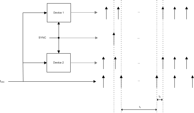
LMX2595 SYNC_Example_snas696.gifFigure 31. Devices Are Now Synchronized to OSCin Signal

When the SYNC feature is enabled, part of the channel divide may be included in the feedback path. This will be referred to as IncludedDivide

Table 12. IncludedDivide With VCO_PHASE_SYNC = 1

OUTx_MUX CHANNEL DIVIDER INCLUDEDDIVIDE
OUTB_MUX = 1 ("VCO")
OUTA_MUX = 1 "VCO" or 2 "VCO Doubler"
Don't Care 1
All Other Valid Conditions Divisible by 3, but NOT 24 or 192 SEG0 × SEG1 = 6
All other values SEG0 × SEG1 = 4
LMX2595 Sync_Functional_Diagram_snas696.gifFigure 32. Phase SYNC Diagram