SNAS736C June   2017  – April 2019 LMX2595

PRODUCTION DATA.  

  1. Features
  2. Applications
  3. Description
    1.     Device Images
      1.      Simplified Schematic
  4. Revision History
  5. Pin Configuration and Functions
    1.     Pin Functions
  6. Specifications
    1. 6.1 Absolute Maximum Ratings
    2. 6.2 ESD Ratings
    3. 6.3 Recommended Operating Conditions
    4. 6.4 Thermal Information
    5. 6.5 Electrical Characteristics
    6. 6.6 Timing Requirements
    7. 6.7 Typical Characteristics
  7. Detailed Description
    1. 7.1 Overview
    2. 7.2 Functional Block Diagram
    3. 7.3 Feature Description
      1. 7.3.1  Reference Oscillator Input
      2. 7.3.2  Reference Path
        1. 7.3.2.1 OSCin Doubler (OSC_2X)
        2. 7.3.2.2 Pre-R Divider (PLL_R_PRE)
        3. 7.3.2.3 Programmable Multiplier (MULT)
        4. 7.3.2.4 Post-R Divider (PLL_R)
        5. 7.3.2.5 State Machine Clock
      3. 7.3.3  PLL Phase Detector and Charge Pump
      4. 7.3.4  N-Divider and Fractional Circuitry
      5. 7.3.5  MUXout Pin
        1. 7.3.5.1 Lock Detect
        2. 7.3.5.2 Readback
      6. 7.3.6  VCO (Voltage-Controlled Oscillator)
        1. 7.3.6.1 VCO Calibration
        2. 7.3.6.2 Determining the VCO Gain
      7. 7.3.7  Channel Divider
      8. 7.3.8  VCO Doubler
      9. 7.3.9  Output Buffer
      10. 7.3.10 Power-Down Modes
      11. 7.3.11 Phase Synchronization
        1. 7.3.11.1 General Concept
        2. 7.3.11.2 Categories of Applications for SYNC
        3. 7.3.11.3 Procedure for Using SYNC
        4. 7.3.11.4 SYNC Input Pin
      12. 7.3.12 Phase Adjust
      13. 7.3.13 Fine Adjustments for Phase Adjust and Phase SYNC
      14. 7.3.14 Ramping Function
        1. 7.3.14.1 Manual Pin Ramping
          1. 7.3.14.1.1 Manual Pin Ramping Example
        2. 7.3.14.2 Automatic Ramping
          1. 7.3.14.2.1 Automatic Ramping Example (Triangle Wave)
      15. 7.3.15 SYSREF
        1. 7.3.15.1 Programmable Fields
        2. 7.3.15.2 Input and Output Pin Formats
          1. 7.3.15.2.1 Input Format for SYNC and SysRefReq Pins
          2. 7.3.15.2.2 SYSREF Output Format
        3. 7.3.15.3 Examples
        4. 7.3.15.4 SYSREF Procedure
      16. 7.3.16 SysRefReq Pin
    4. 7.4 Device Functional Modes
    5. 7.5 Programming
      1. 7.5.1 Recommended Initial Power-Up Sequence
      2. 7.5.2 Recommended Sequence for Changing Frequencies
      3. 7.5.3 General Programming Requirements
    6. 7.6 Register Maps
      1. 7.6.1  General Registers R0, R1, & R7
        1. Table 25. Field Descriptions
      2. 7.6.2  Input Path Registers
        1. Table 26. Field Descriptions
      3. 7.6.3  Charge Pump Registers (R13, R14)
        1. Table 27. Field Descriptions
      4. 7.6.4  VCO Calibration Registers
        1. Table 28. Field Descriptions
      5. 7.6.5  N Divider, MASH, and Output Registers
        1. Table 29. Field Descriptions
      6. 7.6.6  SYNC and SysRefReq Input Pin Register
        1. Table 30. Field Descriptions
      7. 7.6.7  Lock Detect Registers
        1. Table 31. Field Descriptions
      8. 7.6.8  MASH_RESET
        1. Table 32. Field Descriptions
      9. 7.6.9  SysREF Registers
        1. Table 33. Field Descriptions
      10. 7.6.10 CHANNEL Divider And VCO Doubler Registers
        1. Table 34. Field Descriptions
      11. 7.6.11 Ramping and Calibration Fields
        1. Table 35. Field Descriptions
      12. 7.6.12 Ramping Registers
        1. 7.6.12.1 Ramp Limits
          1. Table 36. Field Descriptions
        2. 7.6.12.2 Ramping Triggers, Burst Mode, and RAMP0_RST
          1. Table 37. Field Descriptions
        3. 7.6.12.3 Ramping Configuration
          1. Table 38. Field Descriptions
      13. 7.6.13 Readback Registers
        1. Table 39. Field Descriptions
  8. Application and Implementation
    1. 8.1 Application Information
      1. 8.1.1 OSCin Configuration
      2. 8.1.2 OSCin Slew Rate
      3. 8.1.3 RF Output Buffer Power Control
      4. 8.1.4 RF Output Buffer Pullup
      5. 8.1.5 Performance Comparison Between 1572 (0x0624) and 3115 (0x0C2B) for Register DBLR_IBIAS_CTRL1 (R25[15:0])
    2. 8.2 Typical Application
      1. 8.2.1 Design Requirements
      2. 8.2.2 Detailed Design Procedure
      3. 8.2.3 Application Curve
  9. Power Supply Recommendations
  10. 10Layout
    1. 10.1 Layout Guidelines
    2. 10.2 Layout Example
  11. 11Device and Documentation Support
    1. 11.1 Device Support
      1. 11.1.1 Third-Party Products Disclaimer
      2. 11.1.2 Development Support
    2. 11.2 Documentation Support
      1. 11.2.1 Related Documentation
    3. 11.3 Receiving Notification of Documentation Updates
    4. 11.4 Community Resources
    5. 11.5 Trademarks
    6. 11.6 Electrostatic Discharge Caution
    7. 11.7 Glossary
  12. 12Mechanical, Packaging, and Orderable Information

RF Output Buffer Pullup

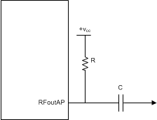
The choice of output buffer components is very important and can have a profound impact on the output power. Table 40 shows how to treat each pin. If using a single-ended output, a pullup is required, and the user can put a 50-Ω resistor after the capacitor.

Table 40. Different Methods for Pullup on Outputs

PULLUP STYLE DIAGRAM COMMENTS
Inductor LMX2595 ai_output_ind_snas696.gif Potentially higher output power, but output impedance is far from 50 Ω. Consider also using with a resistive pad.
Resistor LMX2595 ai_output_res_snas696.gif More consistent matching

Table 41. Output Pullup Configuration

COMPONENT VALUE PART NUMBER
Inductor Varies with frequency
Resistor 50 Ω Vishay FC0402E50R0BST1
Capacitor Varies with frequency ATC 520L103KT16T
ATC 504L50R0FTNCFT