SNAS828A february 2022 – june 2023 LMK1D1208I
PRODUCTION DATA
- 1
- 1 Features
- 2 Applications
- 3 Description
- 4 Revision History
- 5 Device Comparison
- 6 Pin Configuration and Functions
- 7 Specifications
- 8 Parameter Measurement Information
- 9 Detailed Description
- 10Application and Implementation
- 11Device and Documentation Support
- 12Mechanical, Packaging, and Orderable Information
9.3.6 Input Termination
The LMK1D1208I inputs can be interfaced with LVDS, LVPECL, HCSL or LVCMOS drivers.
Figure 9-3 and Figure 9-4 show how LVDS drivers can be connected to LMK1D1208I inputs with DC coupling and AC coupling, respectively.
 Figure 9-3 LVDS Clock Driver Connected to LMK1D1208I Input (DC-Coupled)
 Figure 9-4 LVDS Clock Driver Connected to LMK1D1208I Input (AC-Coupled)
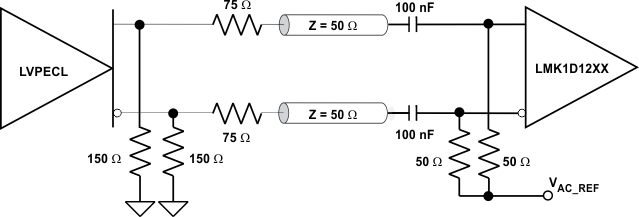
Figure 9-5 shows how to connect LVPECL inputs to the LMK1D1208I. The series resistors are required to reduce the LVPECL signal swing if the signal swing is >1.6 VPP.
 Figure 9-5 LVPECL Clock Driver Connected to LMK1D1208I Input
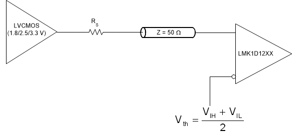
Figure 9-6 shows how to couple a LVCMOS clock input to the LMK1D1208I directly.
 Figure 9-6 1.8-V, 2.5-V, or 3.3-V
LVCMOS Clock Driver Connected to LMK1D1208I Input
Figure 9-6 1.8-V, 2.5-V, or 3.3-V
LVCMOS Clock Driver Connected to LMK1D1208I InputFor unused input, TI recommends grounding both input pins (INP, INN) using 1-kΩ resistors.