SNAU182A March   2021  – May 2022


  1.   Trademarks
  2. 1LMX2571EPEVM Evaluation Module
    1. 1.1 Evaluation Module Contents
    2. 1.2 Evaluation Setup Requirement
    3. 1.3 Resources
  3. 2Setup
    1. 2.1 Connection Diagram
    2. 2.2 Power Supply
    3. 2.3 Reference Clock
    4. 2.4 RF Output
    5. 2.5 Programming
    6. 2.6 Evaluation Software
    7. 2.7 EVM Strap Options
      1. 2.7.1 J11 Header
      2. 2.7.2 J12 Header
  4. 3Typical Measurement
    1. 3.1 Default Configuration
      1. 3.1.1 Loop Filter
      2. 3.1.2 Typical Output
    2. 3.2 Additional Tests
      1. 3.2.1 FSK Modulation
      2. 3.2.2 Register Readback
  5. 4Schematic
  6. 5Board Construction
    1. 5.1 PCB Layer Stack-Up
    2. 5.2 PCB Layout
  7. 6Bill of Materials
  8. 7Troubleshooting Guide
  9.   A Using Different Reference Clock
  10.   B Reference PRO
    1.     B.1 Output Frequency Selection
    2.     B.2 Output Format Selection
    3.     B.3 Typical Output Characteristics
    4.     B.4 Firmware Update
  11.   C Revision History

FSK Modulation

Direct digital FSK modulation is supported in LMX2571. FSK PIN mode supports discrete 2-, 4-, or 8-level FSK modulation while other FSK modes support arbitrary level FSK modulation. Table 3-2 is an FSK PIN mode example.

Table 3-2 FSK PIN Mode Example
PARAMETER EXAMPLE VALUE
Phase detector frequency 80 MHz
CHDIV1 Divided by 4
CHDIV2 Divided by 1
PLL_DEN 224
Prescalar 2
Frequency deviation ±600 Hz; ±1800 Hz

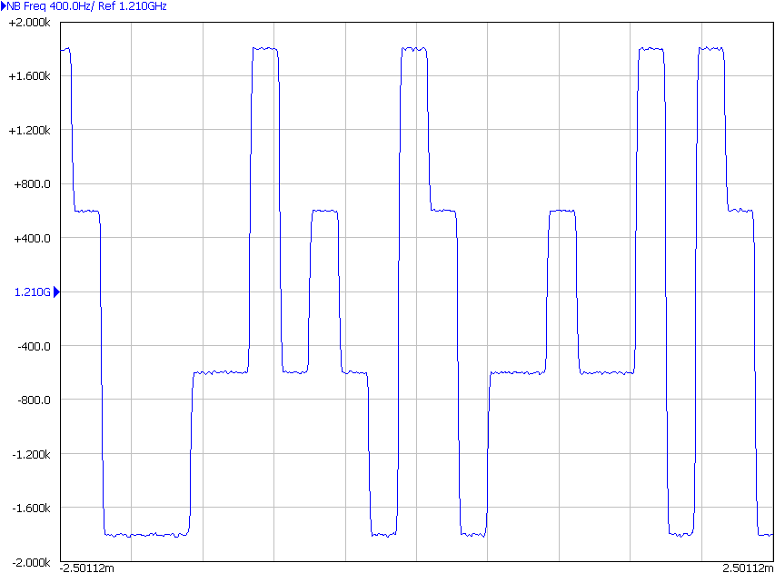
Continue to toggle the FSK_D[1:0] and FSK_DV pins, the output is a discrete 4-level FSK modulated signal.
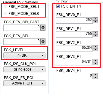
GUID-A1874FA3-368B-4CFA-B27C-AE8AA76F6676-low.png Figure 3-3 FSK PIN Mode Setting
GUID-2323143D-F511-4F0A-91B6-A64ED2701BFE-low.png Figure 3-4 FSK PIN Mode