-
LMK5C33216EVM User's Guide
- Trademarks
- 1Introduction
- 2EVM Quick Start
- 3EVM Configuration
-
4EVM Schematics
- 4.1 Power Supply Schematic
- 4.2 Power Distribution Schematic
- 4.3 LMK5C33216 and Input Reference Inputs IN0 to IN1 Schematic
- 4.4 Clock Outputs OUT0 to OUT3 Schematic
- 4.5 Clock Outputs OUT4 to OUT9 Schematic
- 4.6 Clock Outputs OUT10 to OUT15 Schematic
- 4.7 XO Schematic
- 4.8 Logic I/O Interfaces Schematic
- 4.9 USB2ANY Schematic
- 5EVM Bill of Materials
- 6Appendix A - TICS Pro LMK5C33216 Software
- 7Revision History
- IMPORTANT NOTICE
LMK5C33216EVM User's Guide
Trademarks
All trademarks are the property of their respective owners.
1 Introduction
Overview
The LMK5C33216EVM is an evaluation module for the LMK5C33216 Network Clock Generator and Synchronizer. The EVM can be used for device evaluation, compliance testing, and system prototyping. The LMK5C33216 integrates three Analog PLLs (APLL) and three Digital PLLs (DPLL) with programmable loop bandwidth. The EVM includes SMA connectors for clock inputs, oscillator inputs, and clock outputs to interface the device with 50-Ω test equipment.
The onboard TCXO allows the LMK5C33216 to be evaluated in free-running, locked, or holdover mode of operation. The EVM can be configured through the onboard USB microcontroller (MCU) interface using a PC with TI's TICS Pro software graphical user interface (GUI). TICS Pro can be used to program the LMK5C33216 registers.
Features
- LMK5C33216 DUT
What is Included
- LMK5C33216EVM
What is Needed
- Windows PC with TICS Pro Software GUI
- Test Equipment
- DC power supply (5 V, 2 A)
- Real-time oscilloscope
- Source signal analyzer
- Precision frequency counter
- Signal generator / reference clock
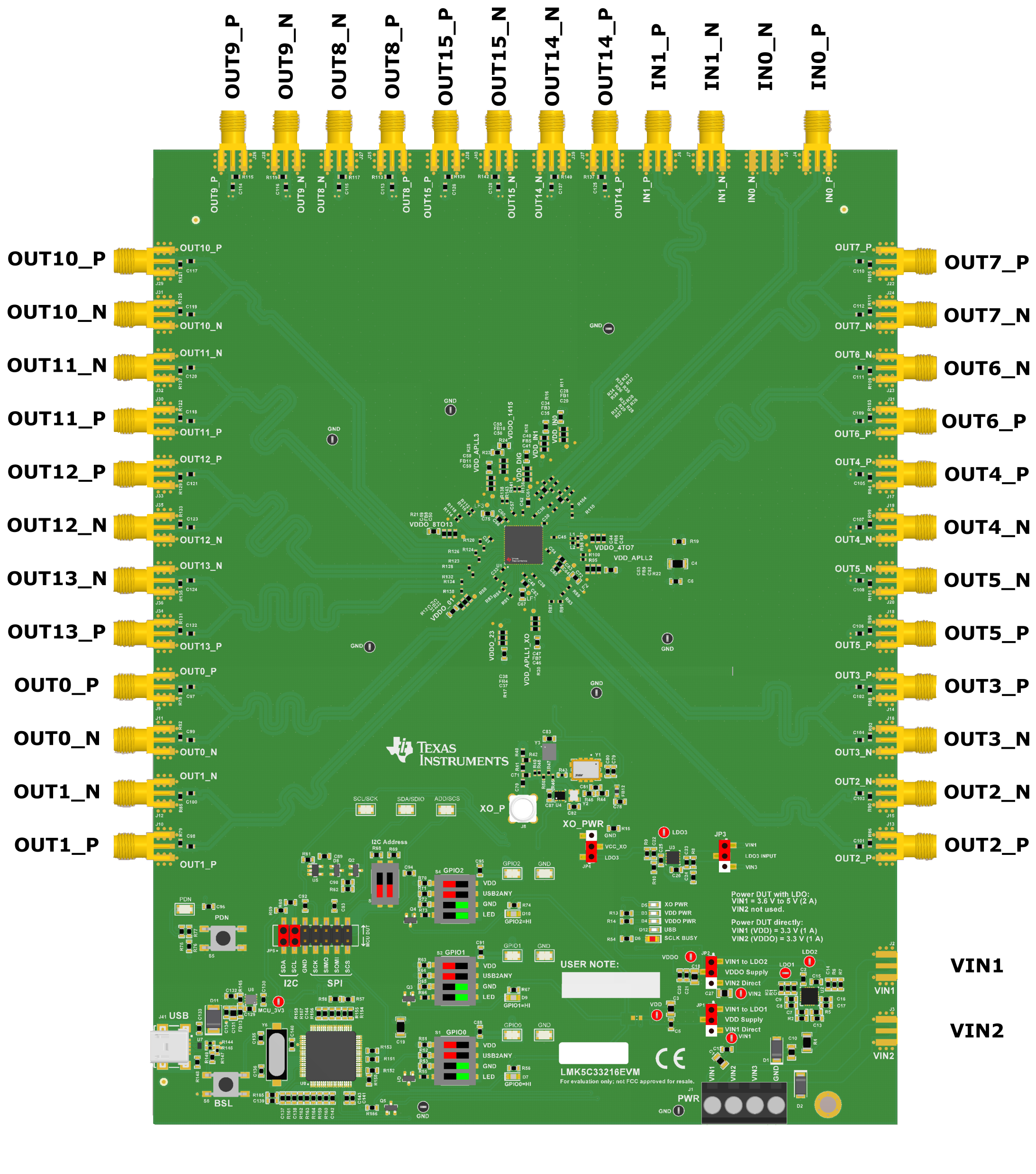
In Figure 1-1, jumper position is shown by the red markings. Dip switch positions are shown be either a green box (for ON) or red box (for OFF) in the appropriate location.
 Figure 1-1 LMK5C33216EVM Default Setting of Jumpers and Dip
Switches
Figure 1-1 LMK5C33216EVM Default Setting of Jumpers and Dip
Switches2 EVM Quick Start
Table 2-1 describes the default jumper positions for the EVM to power the device from a single 4.5 V supply provided to VIN1. In positional information about jumpers, adj des means jumper is placed adjacent to designator. Opp des means jumper is placed opposite designator.
| CATEGORY | REF DES | POSITION | DESCRIPTION | |
|---|---|---|---|---|
| Power |
JP1 |
1-2 (adj des) |
DUT VDD = 3.3 V from LDO1 provided by U3. | |
|
JP2 |
1-2 (adj des) |
DUT VDDO = 3.3 V from LDO2 rail provided by U3. | ||
|
JP3 |
1-2 (adj des) |
LDO3 IN powered from VIN1 external supply. | ||
|
JP4 |
1-2 (adj des) |
XO VCC = 3.3 V from LDO3. | ||
| Communication |
JP5 |
1-2, 3-4 |
Connect I2C from onboard USB2ANY to DUT | |
| LMK5C33216 Control Pins |
S3 |
S5[1:2] = OFF |
SCS_ADD = no pull-up or pull-down. | |
|
S1, S2, S4 |
Sx[1,2] = OFF Sx[3,4] = ON |
Enable 3.9k pull-down on GPIO0, GPIO1, and GPIO2 | ||
To begin using the LMK5C33216, follow the steps below.
Hardware Setup
- Verify the EVM default jumper and DIP switch settings shown in Table 3-1.
- Connect Power, +4.5 V from an external DC power
supply (2-A limit), see Figure 3-2.
- To VIN1 & GND terminals on header J1 (pins 1 and 4), or
- To VIN1 SMA connector J2.
- Connect references.
- 156.25 MHz reference clock to IN0_P/N and/or,
- 10 MHz reference clock to IN1_P/N
- Connect USB cable to USB port at J41.
Software Setup
- If not already installed, install TICS Pro software from TI website: http://ti.com/tool/TICSPRO-SW
- If the MATLAB R2015b (9.0)* 64-bit runtime is not already installed, download and install from MathWorks website. While optional for programming and evaluating the default profile settings, the Matlab Runtime is necessary for any application that needs to modify the DPLL loop filter settings. See https://www.mathworks.com/products/compiler/matlab-runtime.html
- Start TICS Pro software
- Select the LMK5C33216 profile from Select Device → Network Synchronizer Clock (Digital PLLs) → LMK5C33216
- Confirm communications with board by
- From the menu bar, click USB communications.
- Click Interface
- In Communication Setup pop-up
window.
- Ensure USB2ANY is selected as the interface.
- In case of multiple USB2ANY, select desired interface. If a USB2ANY is currently in use in another TICS Pro, you must release that interface by changing its interface setting to DemoMode
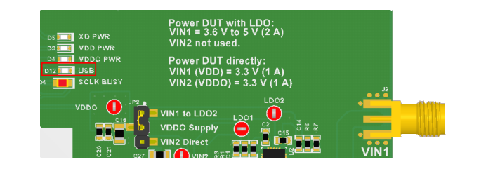
- Click identify to blink LED illustrated in Figure 2-1. This confirms you are connected to the board you expect.
 Figure 2-1 USB LED
Program LMK5C33216
- Toggle switch S5 (PDN/RESET).
- Program all the registers by…
- Pressing Write All Regs button in toolbar
- From the menu bar click USB Communications then click Write All Registers, or
- Pressing Ctrl + L.
- Current consumption should be approximately 1.15 A.
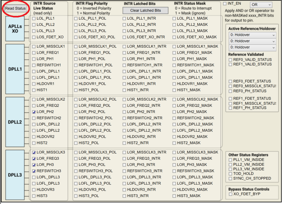
- Check LMK5C33216 Status
- Status Page of GUI
- Click Read Status Bits
- To clear latched bits.
- Press Clear Latched Bits button
- Read Status Bits
- It may take some time for the DPLL status bits to reflect lock.
 Figure 2-2 Read Status Bits
Measure
Measurements may now be made at the clock outputs.
3 EVM Configuration
The LMK5C33216 is a highly configurable clock chip with multiple power domains, PLL domains, and clock input and output domains. To support a wide range of LMK5C33216 use cases, the EVM was designed with more flexibility and functionality than needed to implement the chip in a customer system application.
This section describes the power, logic, and clock input and output interfaces on the EVM, as well as how to connect, set up, and operate the EVM. Refer to Figure 4-1.
| ITEM NO. | REF DES | DESCRIPTION | |
|---|---|---|---|
| 1 | U1 | LMK5C33216 DUT | |
| 2 | A | J1 (VIN1 terminal block header), or | External Supply, +5 V using default configuration. |
| B | J2 (VIN1 SMA) Not populated by default | ||
| 3 | A | Y1, or | |
| B | J8 | ||
| 4 | J4/5, J6/7 | SMA Ports for DUT Clock Inputs (IN0_P/N and IN1_P/N) | |
| 5 | J9/11, J10/12, J13/15, J14/16, J17/19, J18/20, J21/J23, J22/24, J25/27, J26/28, J29/31, J30/32, J33/35, J34/36, J37/39, J38/40 | SMA Ports for DUT Clock Outputs | |
| 6 | S5 | Normally open. Push button for DUT power down (PDN pin). Connect R76 to enable control of the PDN pin through the GUI | |
| 7 | JP5 | Jumper Header for I2C/SPI interface (MCU to DUT) | |
| 8 | D6 | SCL or SCK busy indication LED. | |
| 9 | J41 | USB Port for MCU | |
 Figure 3-1 Key Components - EVM Top
Side