SNAU260A October   2020  – February 2021 LMK5C33216

ADVANCE INFORMATION  

  1.   Trademarks
  2. 1Introduction
  3. 2EVM Quick Start
  4. 3EVM Configuration
    1. 3.1 Power Supply
    2. 3.2 Logic Inputs and Outputs
    3. 3.3 Switching Between I2C and SPI
    4. 3.4 Generating SYSREF Request
    5. 3.5 XO Input
      1. 3.5.1 38.88-MHz TCXO (Default)
      2. 3.5.2 External Clock Input
    6. 3.6 Reference Clock Inputs
    7. 3.7 Clock Outputs
    8. 3.8 Status Outputs and LEDS
    9. 3.9 Requirements for Making Measurements
  5. 4EVM Schematics
    1. 4.1 Power Supply Schematic
    2. 4.2 Power Distribution Schematic
    3. 4.3 LMK5C33216 and Input Reference Inputs IN0 to IN1 Schematic
    4. 4.4 Clock Outputs OUT0 to OUT3 Schematic
    5. 4.5 Clock Outputs OUT4 to OUT9 Schematic
    6. 4.6 Clock Outputs OUT10 to OUT15 Schematic
    7. 4.7 XO Schematic
    8. 4.8 Logic I/O Interfaces Schematic
    9. 4.9 USB2ANY Schematic
  6. 5EVM Bill of Materials
    1. 5.1 Loop Filter and Vibration Nonsensitive Capacitors
  7. 6Appendix A - TICS Pro LMK5C33216 Software
    1. 6.1 Using the Start Page
      1. 6.1.1 Step 1
      2. 6.1.2 Step 2
      3. 6.1.3 Step 3
      4. 6.1.4 Step 4
      5. 6.1.5 Step 5
      6. 6.1.6 Step 6
      7. 6.1.7 Step 7
    2. 6.2 Using the Status Page
    3. 6.3 Using the Input Page
      1. 6.3.1 Cascaded Configurations
        1. 6.3.1.1 Cascade VCO to APLL Reference
    4. 6.4 Using APLL1, 2, and 3 Pages
    5. 6.5 Using the DPLL1, 2, and 3 Pages
      1. 6.5.1 DPLL DCO
    6. 6.6 Using the Validation Page
    7. 6.7 Using the GPIO Page
    8. 6.8 Using the Outputs Page
  8. 7Revision History

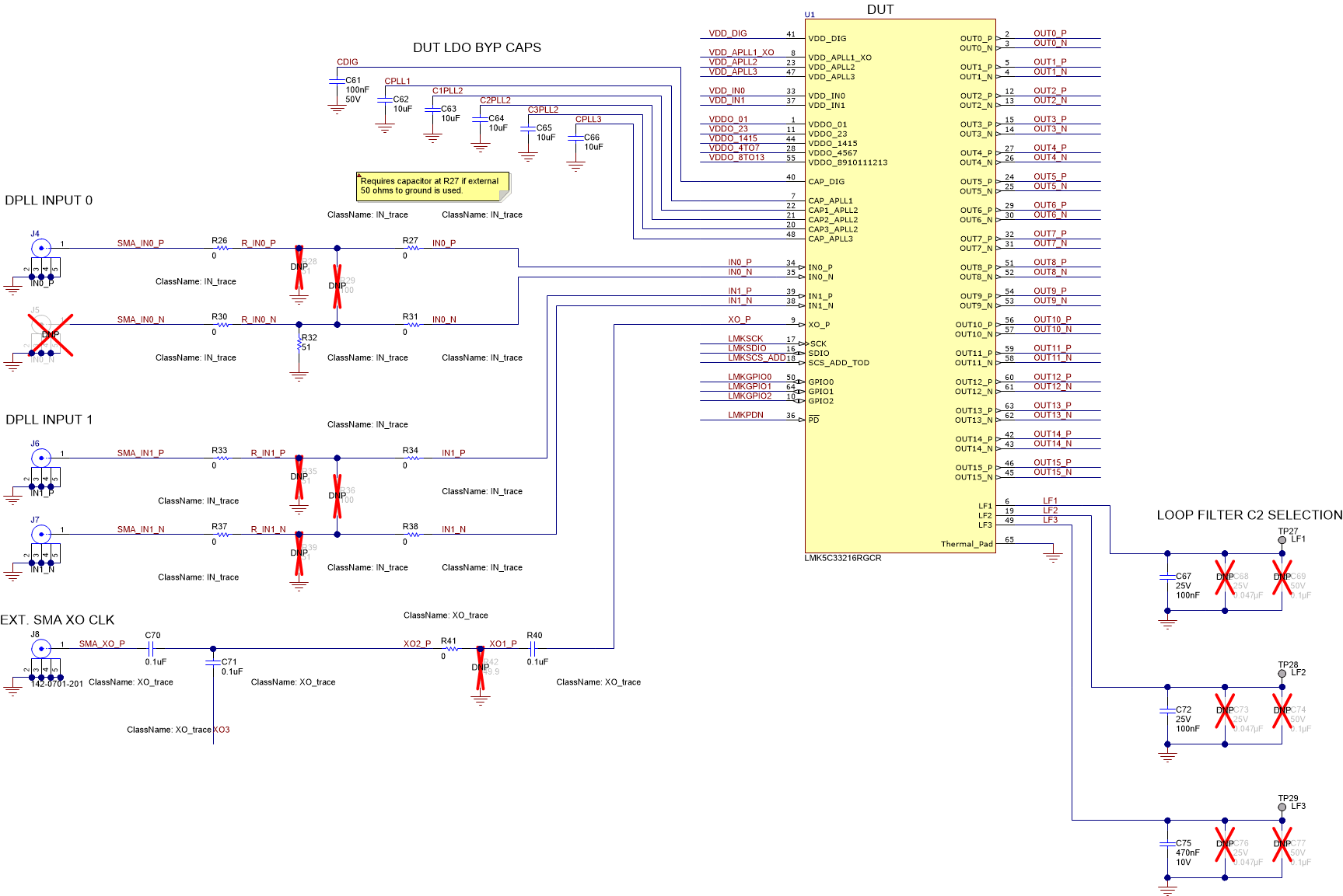
LMK5C33216 and Input Reference Inputs IN0 to IN1 Schematic

GUID-20201014-CA0I-D1DJ-G2DX-JQPXC6DCZWMB-low.gif Figure 4-3 LMK5C33216 and Input Reference Inputs IN0 to IN1