SNAU260A October 2020 – February 2021 LMK5C33216
ADVANCE INFORMATION
- Trademarks
- 1Introduction
- 2EVM Quick Start
- 3EVM Configuration
-
4EVM Schematics
- 4.1 Power Supply Schematic
- 4.2 Power Distribution Schematic
- 4.3 LMK5C33216 and Input Reference Inputs IN0 to IN1 Schematic
- 4.4 Clock Outputs OUT0 to OUT3 Schematic
- 4.5 Clock Outputs OUT4 to OUT9 Schematic
- 4.6 Clock Outputs OUT10 to OUT15 Schematic
- 4.7 XO Schematic
- 4.8 Logic I/O Interfaces Schematic
- 4.9 USB2ANY Schematic
- 5EVM Bill of Materials
- 6Appendix A - TICS Pro LMK5C33216 Software
- 7Revision History
3.5 XO Input
The LMK5C33216 has an XO input (XO_P pin) to accept a reference clock for the Fractional-N APLLs. The XO input determines the output frequency accuracy and stability in free-run or holdover modes. For synchronization applications like SyncE or IEEE 1588, the XO input would typically be driven by a low frequency TCXO, OCXO, or external traceable clock that conforms to the frequency accuracy and holdover stability requirements of the application. For DPLL mode, the XO frequency must have a non-integer frequency relationship with the VCO frequency of any APLLs which utilize XO input as their reference. For APLL only mode (DPLL not used), the XO frequency can have an integer relationship with the VCO to avoid fractional spurs. Any APLL may accept any other APLL as a reference instead of the XO. The BAW on APLL3 provides a good option for a high frequency cascaded referenced.
The XO input of the LMK5C33216 has programmable on-chip input termination and AC-coupled input biasing options to support any clock interface type.
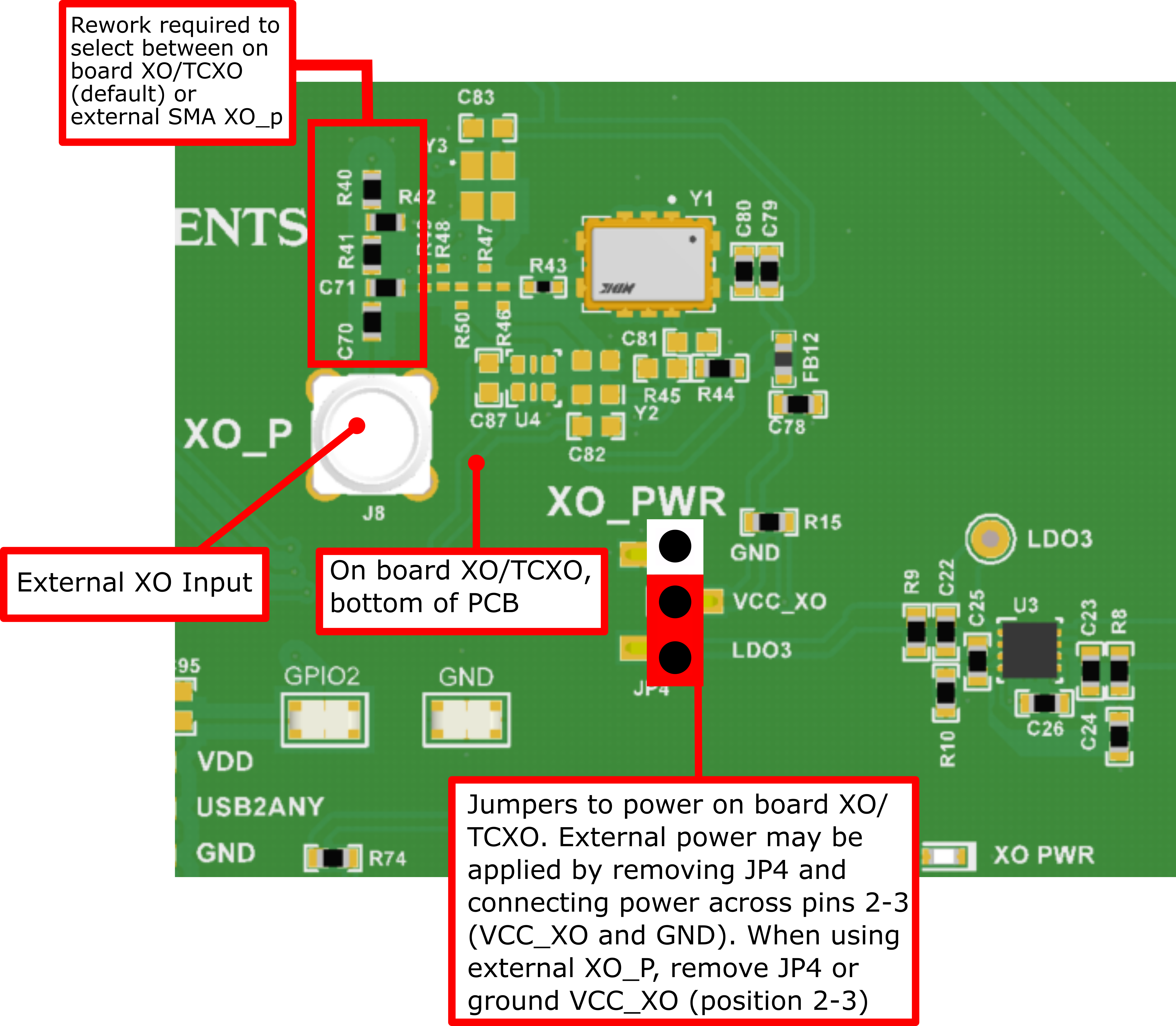
For flexibility, the EVM provides the XO input options (use one at a time). C70 allows an external reference to be provided at SMA connector XO_P (J8). C71 allows one of the on board XO/TCXO/OCXO footprints to be used. By default Y1 is populated with a 38.88 MHz TCXO and selected with the populated R43. Other XO/TCXO/OCXO may be installed and connected using the appropriate resistor. Care should be taken if more than one device is installed to remove resistors for isolation.
 Figure 3-10 XO Input