SNAU270 February 2022 LMK1D1208I
8.1 I2C Address Selection
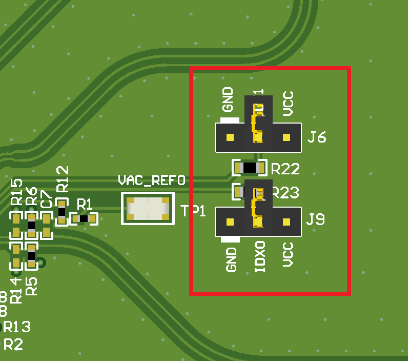
The LMK1D1208I can be configured among four different I2C addresses by setting the two-level IDX pins. Jumpers, J9 and J6, are routed to the IDX0 and IDX1 pins and can be connected to VDD or GND. Use Table 8-1 to determine the appropriate jumper layout to select the I2C address.
Table 8-1 I2C Address Assignment
| I2C ADDRESS | IDX1 | IDX0 |
|---|---|---|
| 0x68 | GND | GND |
| 0x69 | GND | VDD |
| 0x6A | VDD | GND |
| 0x6B | VDD | VDD |
 Figure 8-4 I2C Address Selection
Layout.