SNAU270 February 2022 LMK1D1208I
8 Using I2C
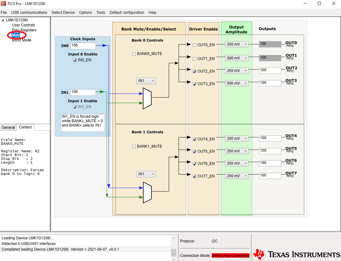
The user can program the LMK1D1208I through the TICSPRO software (available for download on ti.com). This GUI allows the user to control the input enables, bank enable/mute controls, individual output enable, and individual output amplitude.
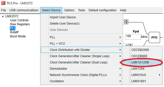
From the TICS Pro toolbar located at the top, click Select Device → Clock Distribution with Divider → LMK1D1208I to access the profile.
 Figure 8-1 Locate the LMK1D1208I Device Profile.
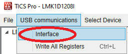
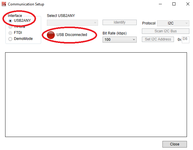
 Using the same toolbar, click USB communications → Interface → USB2ANY to switch from DemoMode to I2C.

 Figure 8-2 Set to I2C Communication.
 TI highly recommends that the user only modifies the registers available in the Main tab. Using the LMK1D1208I beyond logic states allowed in the GUI should be avoided to ensure performance and prevent device misuse.
 Figure 8-3 LMK1D1208I GUI Main Page.