SNAU277C April   2022  – October 2024 LMK6C , LMK6D , LMK6H , LMK6P


  1.   1
  2.   Description
  3.   Features
  4.   4
  5. 1Evaluation Module Overview
    1. 1.1 Introduction
    2. 1.2 Evaluation Module Contents
    3. 1.3 Evaluation Setup Requirement
  6. 2Hardware
    1. 2.1 Setup
      1. 2.1.1 Connection Diagram
      2. 2.1.2 Power Supply
      3. 2.1.3 Clock Output
      4. 2.1.4 EVM Strap Options
        1. 2.1.4.1 J1 Header
        2. 2.1.4.2 J2 Header
        3. 2.1.4.3 J3 Header
        4. 2.1.4.4 J4 Header
        5. 2.1.4.5 J6 Header
        6. 2.1.4.6 J7 Header
        7. 2.1.4.7 J8 Header
      5. 2.1.5 Configuring the Clock Output Termination
  7. 3Implementation Results
    1. 3.1 Typical Measurement
      1. 3.1.1 Phase Noise
  8. 4Hardware Design Files
    1. 4.1 Schematics
    2. 4.2 PCB Layout and Layer Stack-Up
      1. 4.2.1 PCB Layer Stack-Up
      2. 4.2.2 PCB Layout
    3. 4.3 Bill of Materials
  9. 5Additional Information
    1. 5.1 Trademarks
  10. 6References
  11. 7Revision History

Connection Diagram

Figure 2-1 shows the LMK6EVM (DCC222A) connection diagram. To test LMK6xDLF variants (DLF 2.5mm × 2.0mm package), the device must be soldered on Y1, and P1 and P2 can be connected to an oscilloscope or phase noise analyzer to evaluate the device output. Similarly for LMK6xDLE variants (DLE 3.2mm × 2.5mm package), the device must be soldered on Y2, and P3 and P4 used accordingly to measure the output. Note that for LMK6C variants with an LVCMOS output format, only the positive clock output connection is used. The 4-pin LMK6C variants can share the same footprint as the 6-pin LMK6D/P/H variants. The corner pins are shared, but the middle pins are left unused for the LMK6C devices.
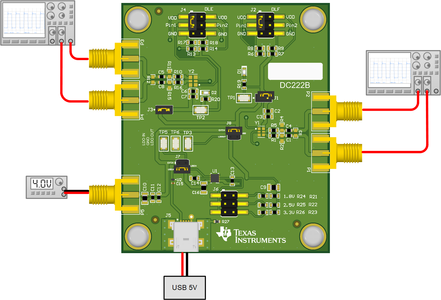
LMK6EVM, LMK6C, LMK6D, LMK6H, LMK6P Connection DiagramFigure 2-1 Connection Diagram