SNAU279A July 2022 – September 2022
- Abstract
- Trademarks
- 1Introduction
- 2EVM Quick Start
- 3EVM Configuration
-
4EVM
Schematics
- 4.1 Power Supply Schematic
- 4.2 Alternative Power Supply Schematic
- 4.3 Power Distribution Schematic
- 4.4 LMK5B33414 and Input Reference Inputs IN0 to IN1 Schematic
- 4.5 Clock Outputs OUT0 to OUT3 Schematic
- 4.6 Clock Outputs OUT4 to OUT9 Schematic
- 4.7 Clock Outputs OUT10 to OUT13 and Clock Inputs IN2 and IN3 Schematic
- 4.8 XO Schematic
- 4.9 Logic I/O Interfaces Schematic
- 4.10 USB2ANY Schematic
- 5EVM Bill of Materials
-
6Appendix A - TICS Pro LMK5B33414 Software
- 6.1 Using the Start Page
- 6.2 Using the Status Page
- 6.3 Using the Input Page
- 6.4 Using APLL1, APLL2, and APLL3 Pages
- 6.5 Using the DPLL1, DPLL2, and DPLL3 Pages
- 6.6 Using the Validation Page
- 6.7 Using the GPIO Page
- 6.8 SYNC/SYSREF/1-PPS Page
- 6.9 Using the Outputs Page
- 6.10 EEPROM Page
- 6.11 Design Report Page
- 7Revision History
2 EVM Quick Start
Table 2-1 describes the default jumper positions for the EVM to power the device from a single 12-V supply provided to VIN4. In positional information about jumpers, "opposite designator” means the jumper is placed opposite of the silkscreen designator.
| CATEGORY | REFERENCE DESIGNATOR | POSITION | DESCRIPTION |
|---|---|---|---|
Power | JP1 | 1-2 (opposite designator) | LMK5B33414 VDD = 3.3 V from DCDC1 provided by U500 on top of the PCB. |
JP2 | 1-2 (opposite designator) | LMK5B33414 VDDO = 3.3 V from DCDC1 provided by U500 on top of the PCB. | |
JP4 | 1-2 (opposite designator) | XO VCC = 3.3 V DCDC1 provided by U500 on top of PCB. | |
Communication | JP5 | 1-2, 3-4 | Connect I2C from onboard USB2ANY to LMK5B33414 |
LMK5B33414 Control Pins | S3 | S3[1:2] = OFF | SCS_ADD = no pullup or pulldown. |
S1, S2, S4 | Sx[1,2] = OFF Sx[3,4] = ON | Enable 3.9 kΩ pulldown on GPIO0, GPIO1, and GPIO2 |
To begin using the LMK5B33414, follow the steps below.
Hardware Setup
- Verify the EVM default jumper and DIP switch settings shown in Figure 1-1.
- Connect the 12-V external power DC power supply (1-A limit) to:
- VIN4 and GND terminals on header J500 (pins 4 and 5, see Figure 3-2.)
- Connect references:
- 25-MHz reference clock to IN0_P/N and/or,
- 25-MHz reference clock to IN1_P/N
- Connect the USB cable to the USB port at J41.
Software Setup
- If not already installed, install the TICS Pro software from the TI website: TICS Pro Software
- If the MATLAB R2015b (9.0)* 64-bit Runtime is not already installed, download and install the software from the MathWorks website. While optional for programming and evaluating the default profile settings, Matlab Runtime is necessary for any application that needs to modify the DPLL loop filter settings. See Matlab Runtime.
- Start the TICS Pro software.
- Select the LMK5B33414 profile from Select Device → Network Synchronizer Clock (Digital PLLs) → LMK5B33414.
- Confirm communications with the board by:
- Click USB communications from the menu bar.
- Click Interface to launch the Communication Setup pop-up window.
- Check these fields in the Communication Setup pop-up window:
- Ensure USB2ANY is selected as the interface.
- In case of multiple USB2ANY, select desired interface. If a USB2ANY is currently in use in another TICS Pro, you must release that interface by changing its interface setting to DemoMode.
- Click Identify to trigger the LED shown in the image below. A blinking LED confirms you are connected to the board you expect. Be aware that USB2ANY devices connected to the PC but not attached to by a TICS Pro instance may blink at a slow rate of 1 second on, 1 second off, continuously. After clicking the Identify button, the LED will flash quickly at about 0.5 seconds on, 0.5 seconds off, for about 5 seconds.
Figure 2-1 USB LED.
Program the LMK5B33414
- Toggle the switch S5 (PDN/RESET).
- Program all the registers:
- Press the Write All Regs button in the toolbar.
- Select USB Communications in the menu bar, then select Write All Registers, or press Ctrl + L.
- Check the current consumption.
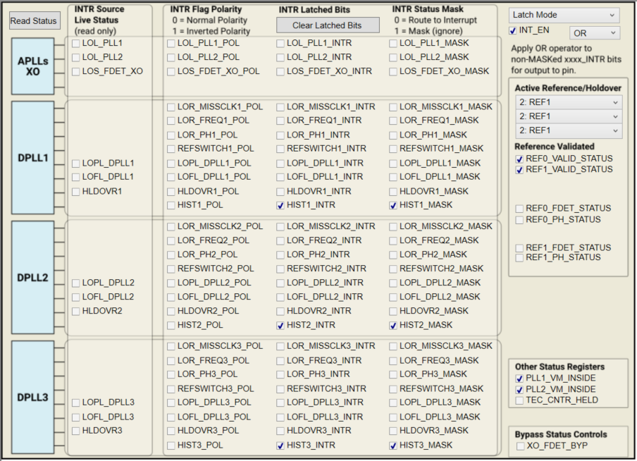
- Check LMK5B33414 Status as shown in Figure 2-2.
- Go to the Status page of the GUI.
- Click Read Status Bits.
- Make sure to clear the latched bits. To clear latched bits:
- Press the Clear Latched Bits button.
- Select Read Status Bits.
- Wait to confirm the change. It may take some time for the DPLL status bits to reflect lock.
 Figure 2-2 Read Status Bits.
 Measure
Measurements can now be made at the clock outputs.