SNAU282 September 2022
- Abstract
- Trademarks
- 1Evaluation Board Kit Contents
- 2Quick Start
- 3PLL Loop Filters and Loop Parameters
- 4Default TICS Pro Mode
- 5Using TICS Pro to Program the LMK04832-SEP
- 6Evaluation Board Inputs and Outputs
- 7Recommended Test Equipment
- 8Schematics
- 9Bill of Materials
- A USB2ANY Firmware Upgrade
- B TICS Pro Usage
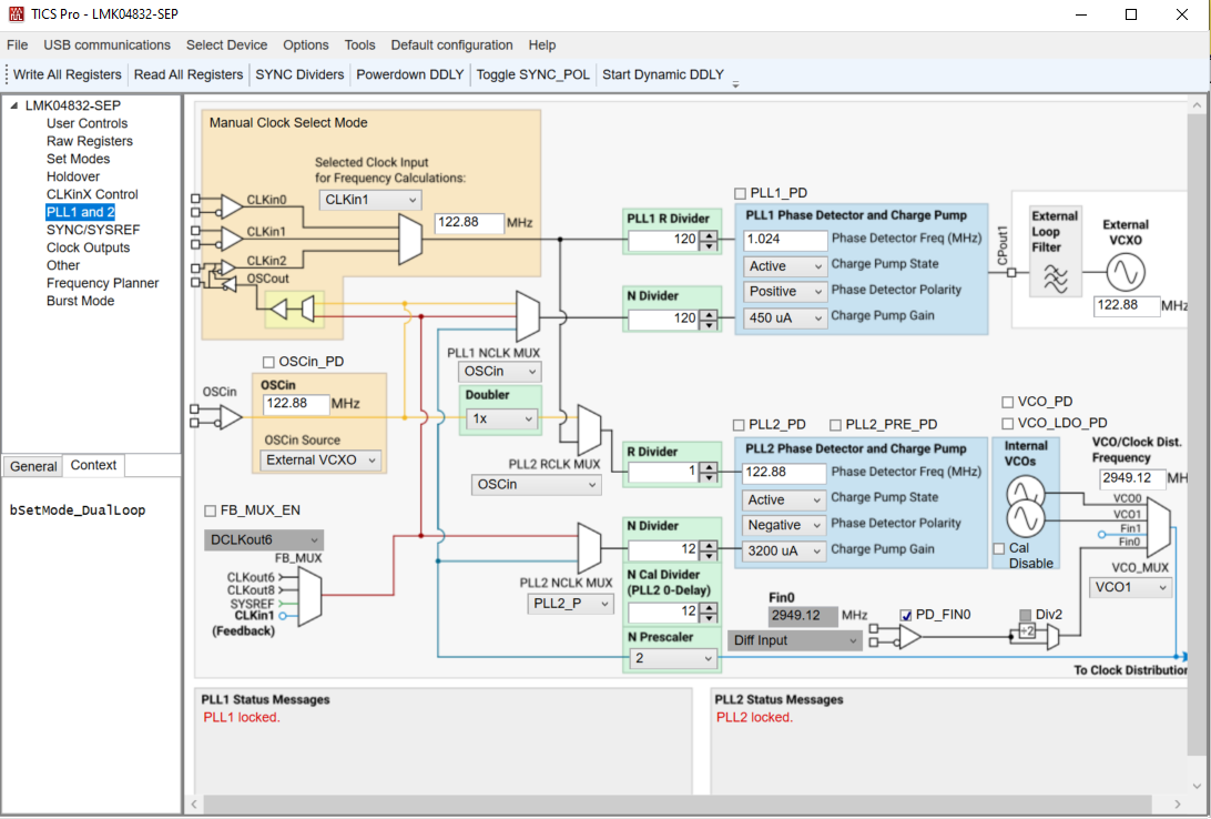
11.7 PLL1 and 2 Page
The PLL1 and 2 page shows the operating frequencies of the PLL1 and PLL2. In distribution mode, the CLKin1 frequency will directly be connected to the VCO/clock distribution path frequency. In addition to the basic PLL dividers and controls, when the PLLX_NCLK_MUX selects the feedback mux as a source, 0-delay modes are achieved. When enabling 0-delay red text will help guide the user through properly setting up 0-delay mode.
When using dual PLL mode, the OSCin Source combo box can be set to External VCXO which links the OSCin frequency with the external VCXO frequency. When using single PLL2 mode, the OSCin Source combo box can be set to Independent to allow the OSCin frequency to be unlinked from the external VCXO frequency.
 Figure 11-7 TICS Pro
- PLL1 and 2 Page