SNAU286 November   2024


  1.   1
  2. 1Description
  3. 2Features
  4.   4
  5. 3Evaluation Module Overview
    1. 3.1 Introduction
    2. 3.2 Kit Contents
    3. 3.3 Specifications
  6. 4Implementation Results
    1. 4.1 Evaluation Setup Requirement
    2. 4.2 Setup
      1. 4.2.1 Connection Diagram
      2. 4.2.2 Power Supply
      3. 4.2.3 Clock Output
      4. 4.2.4 EVM Header Configuration
      5. 4.2.5 Configuring the Output Clock Termination
    3. 4.3 Performance Data and Results
      1. 4.3.1 Typical Measurement
  7. 5Hardware Design Files
    1. 5.1 Schematics
    2. 5.2 PCB Layout and Layer Stack-Up
      1. 5.2.1 PCB Layer Stack-Up
      2. 5.2.2 PCB Layout
    3. 5.3 Bill of Materials
  8. 6Additional Information
    1.     Trademarks
  9. 7Related Documentation

Typical Measurement

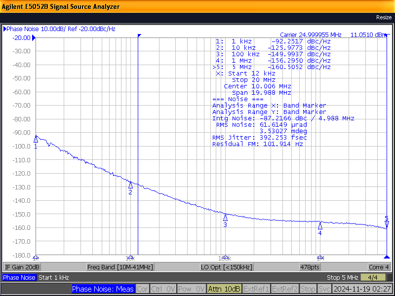
CDC6CEVM Phase Noise Plot of 25MHz
                    CDC6C Variant Figure 4-2 Phase Noise Plot of 25MHz CDC6C Variant
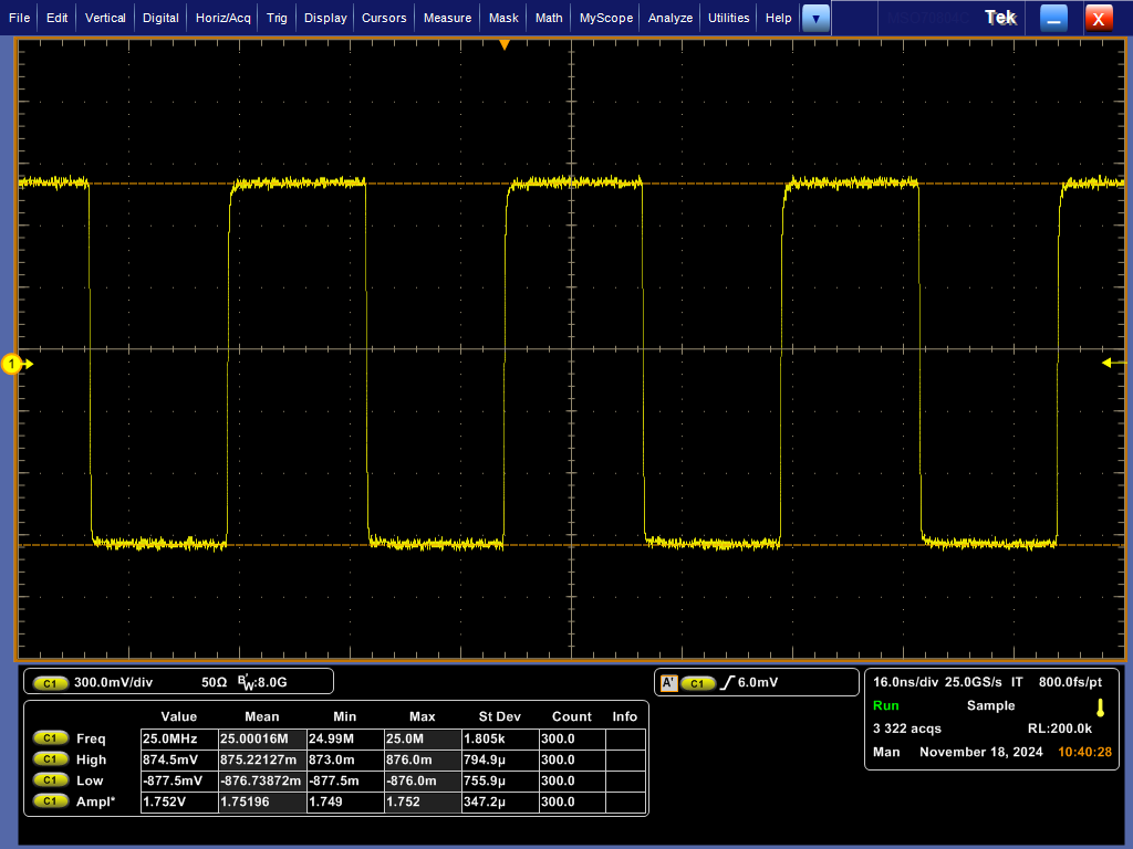
CDC6CEVM Oscilloscope Waveform of 25MHz
                    CDC6C Variant Figure 4-3 Oscilloscope Waveform of 25MHz CDC6C Variant

The output amplitude is reduced from 3.3V to around 1.75V due to the internal 50Ω termination of the oscilloscope