SNAU286 November   2024


  1.   1
  2. 1Description
  3. 2Features
  4.   4
  5. 3Evaluation Module Overview
    1. 3.1 Introduction
    2. 3.2 Kit Contents
    3. 3.3 Specifications
  6. 4Implementation Results
    1. 4.1 Evaluation Setup Requirement
    2. 4.2 Setup
      1. 4.2.1 Connection Diagram
      2. 4.2.2 Power Supply
      3. 4.2.3 Clock Output
      4. 4.2.4 EVM Header Configuration
      5. 4.2.5 Configuring the Output Clock Termination
    3. 4.3 Performance Data and Results
      1. 4.3.1 Typical Measurement
  7. 5Hardware Design Files
    1. 5.1 Schematics
    2. 5.2 PCB Layout and Layer Stack-Up
      1. 5.2.1 PCB Layer Stack-Up
      2. 5.2.2 PCB Layout
    3. 5.3 Bill of Materials
  8. 6Additional Information
    1.     Trademarks
  9. 7Related Documentation

Connection Diagram

Figure 4-1 shows the CDC6CEVM (DCC211A) connection diagram. The top region of the board contains 4 quadrants, one for each package size. Each quadrant contains a footprint to populate a CDC6C oscillator (Y1, Y2, Y3, Y4), a jumper to pull the OE pin high or low (J2, J4), and an output termination network with an SMA connector (P1, P2, P3, P4).

The bottom region of the board contains jumpers for configuring the power supply network. Input power can be provided with the included USB cable, or with an external supply connected to the EXTIN SMA connector.
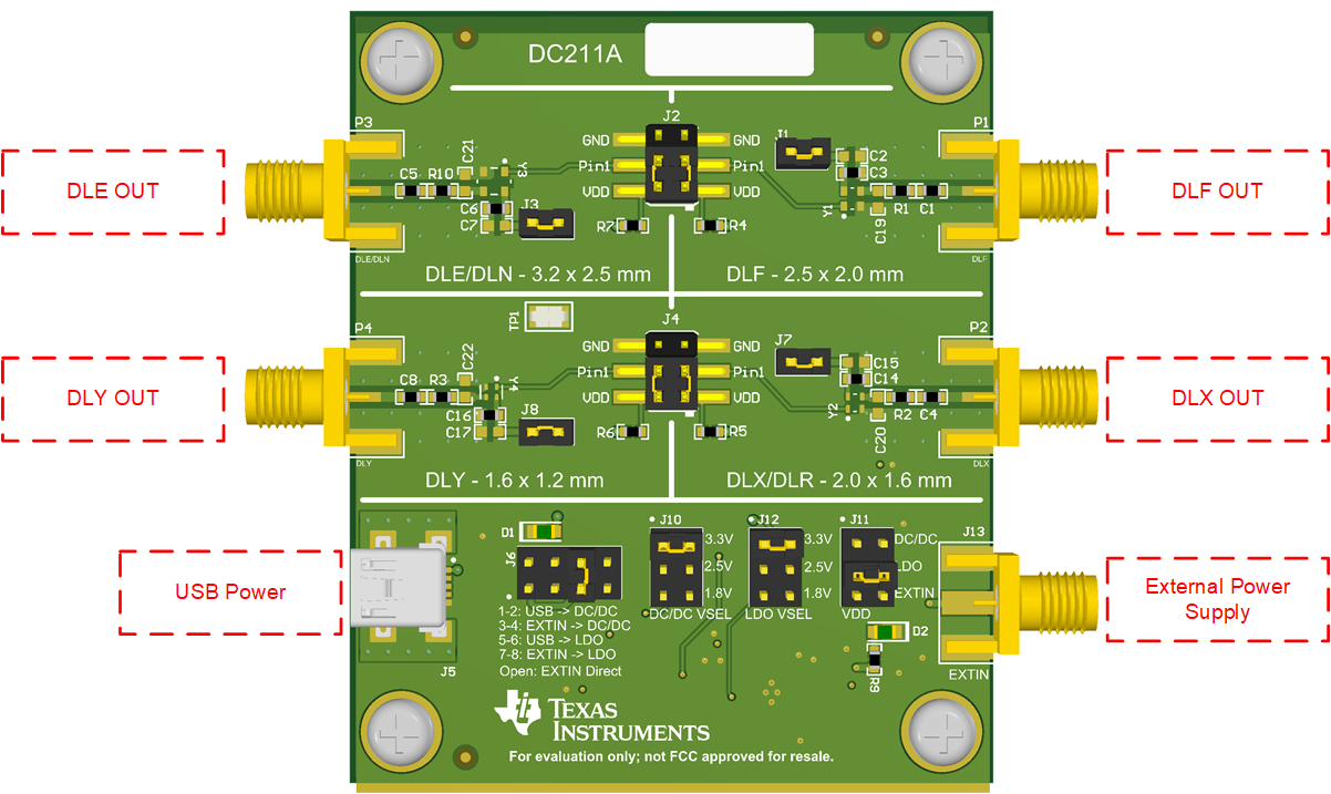
CDC6CEVM Connection DiagramFigure 4-1 Connection Diagram