SNAU287 November 2023
- 1
- Description
- Features
- 4
- 1Evaluation Module Overview
- 2Hardware
- 3Software
- 4Hardware Design Files
- 5Additional Information
- 6Related Documentation
4.2 PCB Layout
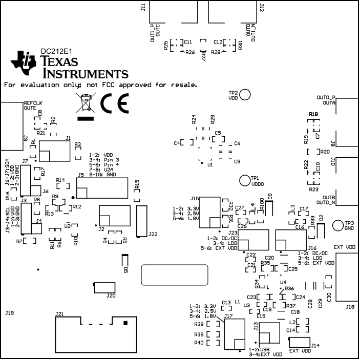 Figure 4-5 Top Overlay
 Figure 4-6 Top Solder Mask
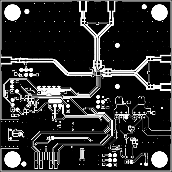 Figure 4-7 Layer 1 (Top Side)
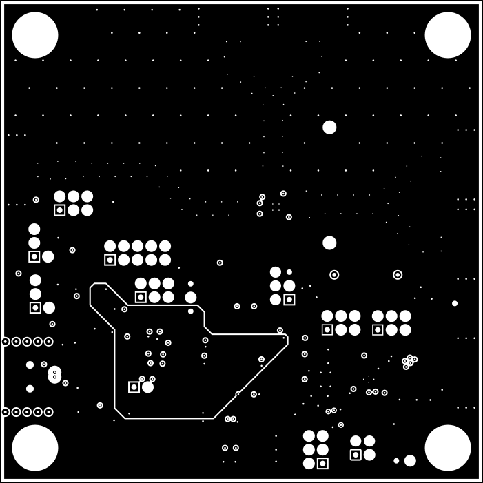 Figure 4-8 Signal Layer 1
 Figure 4-9 Signal Layer 2
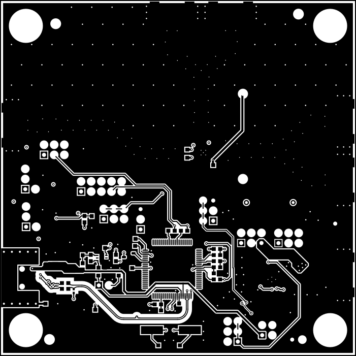 Figure 4-10 Bottom Layer (View from
Top)
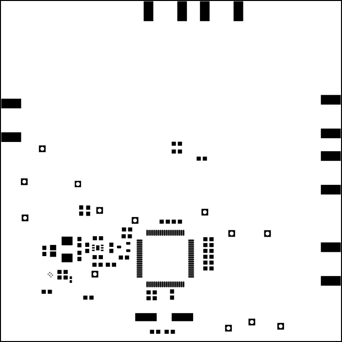 Figure 4-11 Bottom Solder Mask
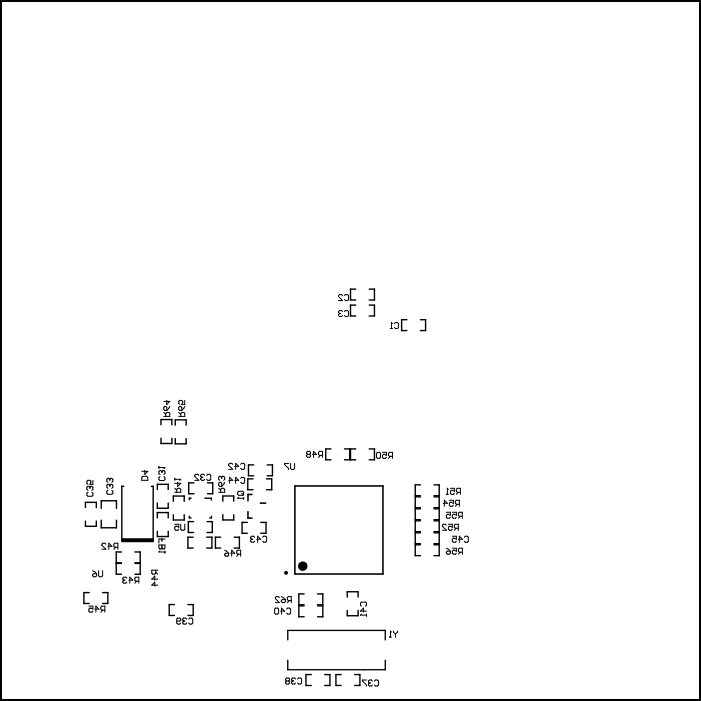 Figure 4-12 Bottom Overlay
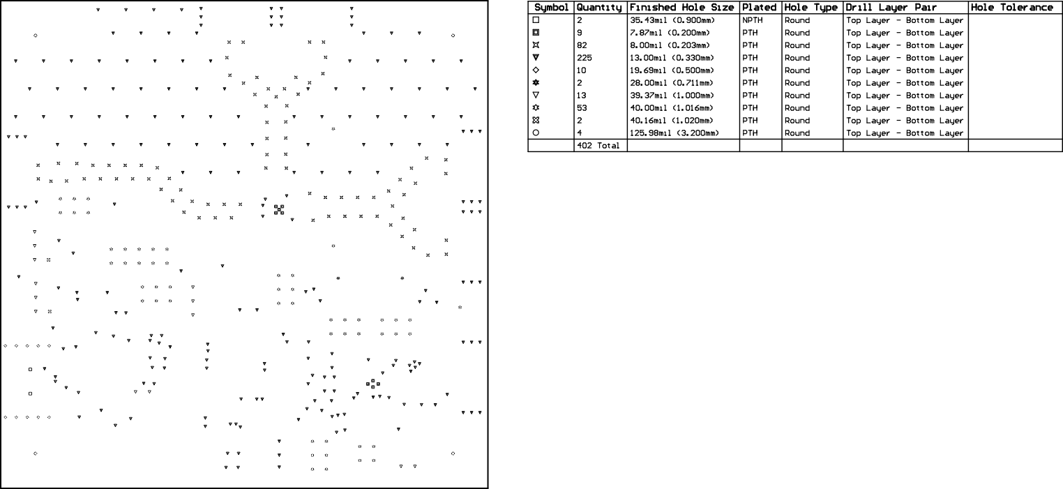 Figure 4-13 Drill Drawing