SNAU293 May 2024 LMX1860-SEP
- 1
- Description
- Features
- Applications
- 5
- 1Evaluation Module Overview
-
2Hardware
- 2.1
Setup
- 2.1.1 Evaluation Setup Requirement
- 2.1.2 Connection Diagram
- 2.1.3 How to Enable Full SPI Control
- 2.1.4 Power Requirements
- 2.1.5 Pin Mode Strapping
- 2.1.6 Reference Clock
- 2.1.7 Output Connections
- 2.1.8 Header Information
- 2.1.9 Default Configuration
- 2.1.10 How to Generate SYSREF
- 2.1.11 Multiplier Mode Example
- 2.1.12 Divider Mode Example
- 2.1.13 Hybrid Mode: SPI and Pin Mode
- 2.1
Setup
- 3Software
- 4Implementation Results
- 5Hardware Design Files
- 6Additional Information
4.1 Buffer, Divider, and Multiplier Modes
From the top-menu, click Default Configuration → 3200MHz Buffer Mode. This automatically loads the buffer mode profile.
 Figure 4-1 Loading the Default
Configuration
Figure 4-1 Loading the Default
ConfigurationAfter the profile is loaded and required any changes have been made, click USB Communications → Write All Registers to program the device.
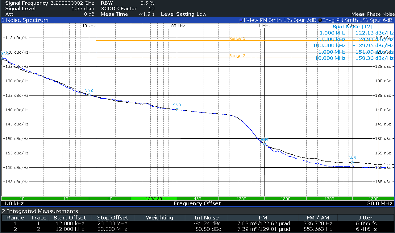
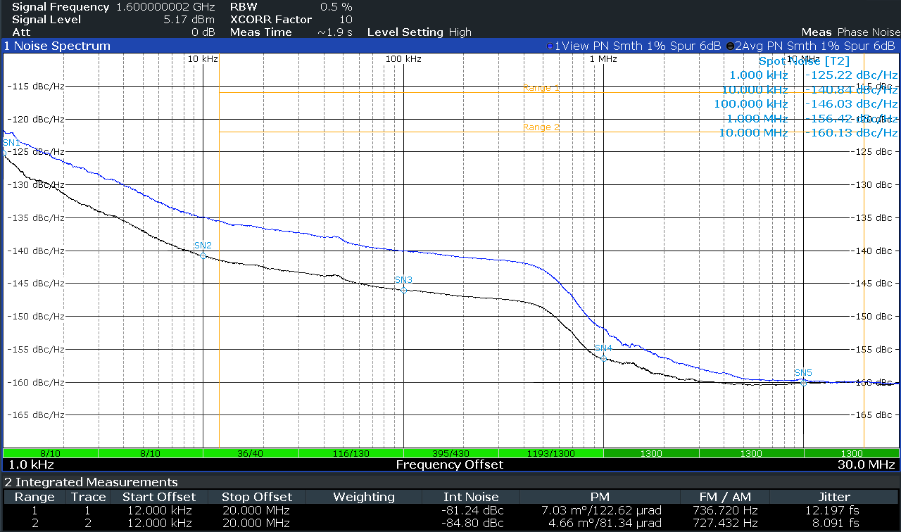
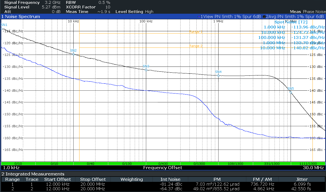
In all of the following plots, the blue trace is the 3.2GHz reference clock from SMA100B and the black trace is the output clock from the device.
 Figure 4-2 Buffer Mode Signal Analyzer
Plot
Figure 4-2 Buffer Mode Signal Analyzer
PlotTo activate the multiplier or the divider, change the CLK_MUX field to specify divider or multiplier modes, and change the CLK_DIV and CLK_MULT fields to specify the frequency scaling factor.
 Figure 4-3 Divide-by-2 Mode Signal
Analyzer Plot
 Figure 4-4 Multiplier x4 Mode Signal
Analyzer Plot