SNAU295
July 2024
LMK5C33216A
1
Abstract
Trademarks
1
Introduction
2
EVM Quick Start
3
EVM Configuration
3.1
Power Supply
3.2
Logic Inputs and Outputs
3.3
Switching Between I2C and SPI
3.4
Generating SYSREF Request
3.5
XO Input
3.5.1
48MHz TCXO (Default)
3.5.2
External Clock Input
3.5.3
Additional XO Input Options
3.5.4
APLL Reference Options
3.6
Reference Clock Inputs
3.7
Clock Outputs
3.8
Status Outputs and LEDS
3.9
Requirements for Making Measurements
3.10
Typical Phase Noise Characteristics
4
EVM Schematics
4.1
Power Supply Schematic
4.2
Alternative Power Supply Schematic
4.3
Power Distribution Schematic
4.4
LMK5C33216A and Input References IN0 to IN1 Schematic
4.5
Clock Outputs OUT0 to OUT3 Schematic
4.6
Clock Outputs OUT4 to OUT9 Schematic
4.7
Clock Outputs OUT10 to OUT15 Schematic
4.8
XO Schematic
4.9
Logic I/O Interfaces Schematic
4.10
USB2ANY Schematic
5
EVM Bill of Materials
5.1
Loop Filter and Vibration Nonsensitive Capacitors
6
Appendix A - TICS Pro LMK5B33216 Software
6.1
Using the Start Page
6.1.1
Step 1
6.1.2
Step 2
6.1.3
Step 3
6.1.4
Step 4
6.1.5
Step 5
6.1.6
Step 6
6.1.7
Step 7
6.2
Using the Status Page
6.3
Using the Input Page
6.3.1
Cascaded Configurations
6.3.1.1
Cascade VCO to APLL Reference
6.4
Using APLL1, APLL2, and APLL3 Pages
6.4.1
APLL DCO
6.5
Using the DPLL1, DPLL2, and DPLL3 Pages
6.5.1
DPLL DCO
6.6
Using the Validation Page
6.7
Using the GPIO Page
6.7.1
SYNC/SYSREF/1-PPS Page
6.8
Using the Outputs Page
6.9
EEPROM Page
6.10
Design Report Page
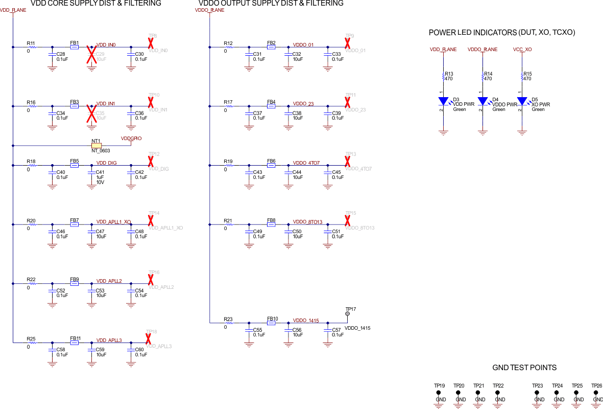
4.3
Power Distribution Schematic
Figure 4-3
Power Distribution