SNAU295 July 2024 LMK5C33216A
- 1
- Abstract
- Trademarks
- 1Introduction
- 2EVM Quick Start
- 3EVM Configuration
-
4EVM Schematics
- 4.1 Power Supply Schematic
- 4.2 Alternative Power Supply Schematic
- 4.3 Power Distribution Schematic
- 4.4 LMK5C33216A and Input References IN0 to IN1 Schematic
- 4.5 Clock Outputs OUT0 to OUT3 Schematic
- 4.6 Clock Outputs OUT4 to OUT9 Schematic
- 4.7 Clock Outputs OUT10 to OUT15 Schematic
- 4.8 XO Schematic
- 4.9 Logic I/O Interfaces Schematic
- 4.10 USB2ANY Schematic
- 5EVM Bill of Materials
- 6Appendix A - TICS Pro LMK5B33216 Software
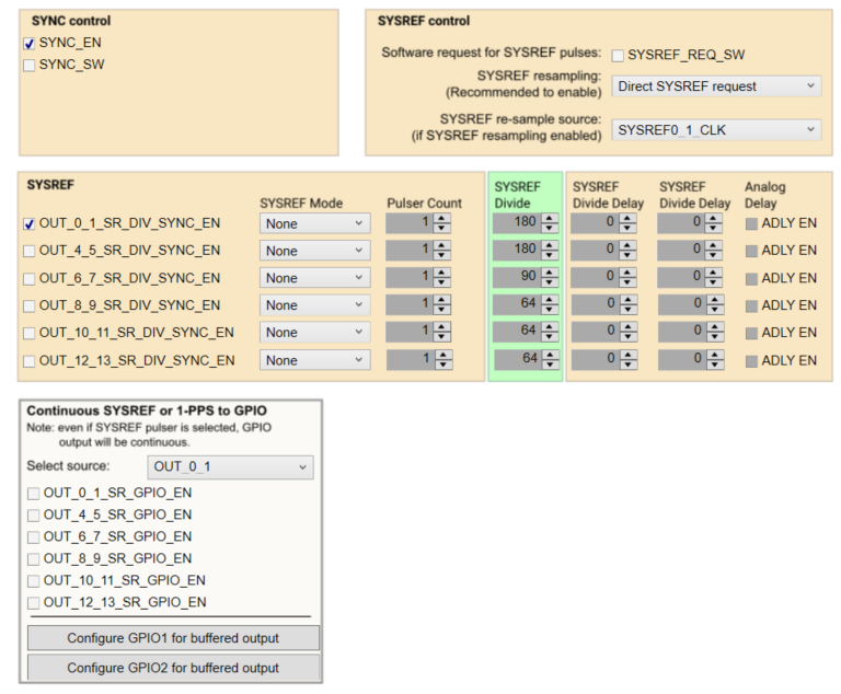
6.7.1 SYNC/SYSREF/1-PPS Page
The SYNC/SYSREF/1-PPS page shows all the SYSREF block settings and allows for a continuous SYSREF or 1-PPS clock to be configured to be outputted from GPIO1 or GPIO2.
The SYSREF divider output signals can be replicated on either GPIO1 and GPIO2 to provide additional single ended 3.3V CMOS clocks after startup if desired. To configure the SYSREF/1PPS output replication, the GPIO must be enabled as an output (GPIOx_OUTEN = 1) and one of the SYSREF output to GPIO replication sources must be active. The SYSREF replication source comes from any one of the SYSREF dividers in use from OUT0/1, OUT4/5, OUT6/7, OUT/9, OUT10/11 or OUT12/13 by register programming (OUT_x_y_SR_GPIO_EN = 1 and GPIO_SYSREF_SEL to the appropriate OUT_x_y). The GPIOx replicated SYSREF output is a continuous frequency. Pulsed SYSREF mode is not supported for the GPIOx replica outputs.
 Figure 6-21 SYNC/SYSREF/1-PPS Page