SNAU303A May   2024  – September 2024


  1.   1
  2.   Description
  3.   Features
  4.   Applications
  5.   5
  6. 1Evaluation Module Overview
    1. 1.1 Introduction
    2. 1.2 Kit Contents
    3. 1.3 Device Information
  7. 2Hardware
    1. 2.1 Setup
      1. 2.1.1 Default Configuration of the LMH1239EVM
      2. 2.1.2 Hardware and Software: Description and Setup
        1. 2.1.2.1 SDI_IN1 Selected
        2. 2.1.2.2 SMBus/I2C Secondary Mode Configuration for the LMH1239EVM GUI
        3. 2.1.2.3 High Level Page for the LMH1239EVM GUI
        4. 2.1.2.4 Eye Monitor for the LMH1239EVM GUI
          1. 2.1.2.4.1 Register Map for the LMH1239EVM GUI
        5. 2.1.2.5 Scripting for the LMH1239EVM GUI
  8. 3Hardware Design Files
    1. 3.1 Schematics
    2. 3.2 PCB Layout
    3. 3.3 Bill of Materials (BOM)
  9. 4Additional Information
    1. 4.1 Trademarks
  10. 5Related Documentation
  11. 6Revision History

PCB Layout

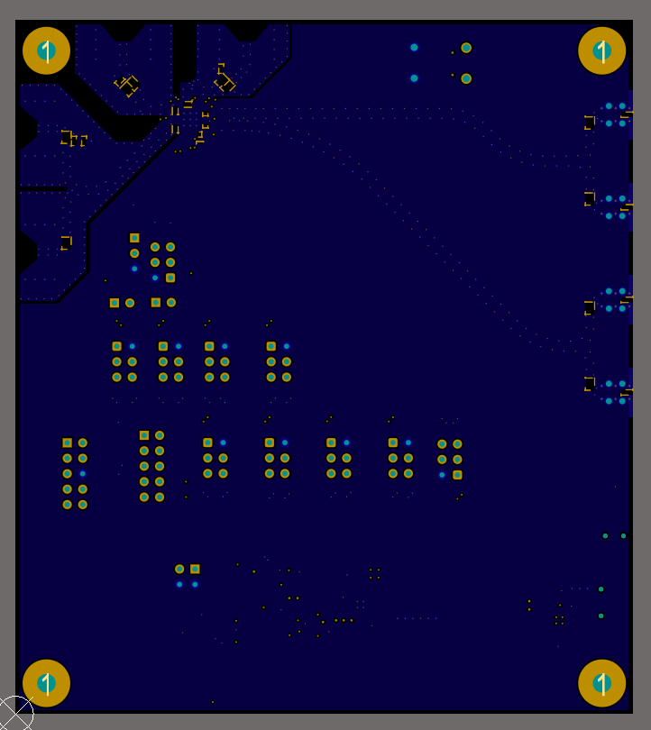
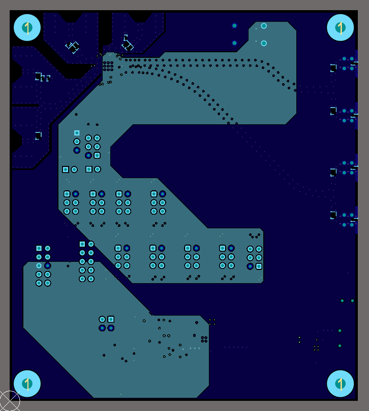
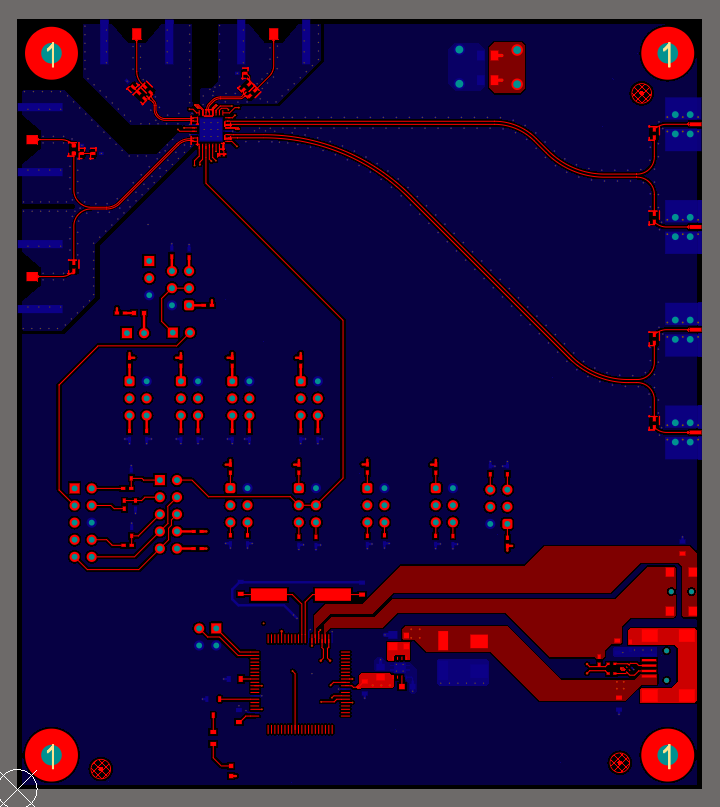
The following figures show the LMH1239EVM layout. The evaluation board controls signal integrity control settings through jumper pins.

The LMH1239EVM allows access to all input channels (SDI_IN and SDI_IN1) and output channels (OUT0, OUT1, and SDI_OUT).
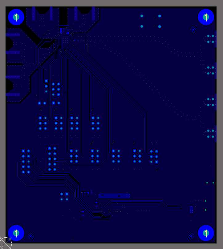
LMH1239EVM LMH1239EVM Bottom LayerFigure 3-2 LMH1239EVM Bottom Layer
LMH1239EVM LMH1239EVM Layer 2 GroundFigure 3-4 LMH1239EVM Layer 2 Ground
LMH1239EVM LMH1239EVM Layer 3 PowerFigure 3-3 LMH1239EVM Layer 3 Power
LMH1239EVM LMH1239EVM Top LayerFigure 3-5 LMH1239EVM Top Layer