SNAU307A May 2024 – May 2024 LMKDB1204
- 1
- Description
- Features
- Applications
- 5
- 1 Evaluation Module Overview
- 2 EVM Quick Start
- 3 Hardware
- 4 Software
- 5 Implementation Results
- 6 Hardware Design Files
- 7 Compliance Information
- 8 Additional Information
- 9 References
- 10Revision History
3.2.3 Clock Input
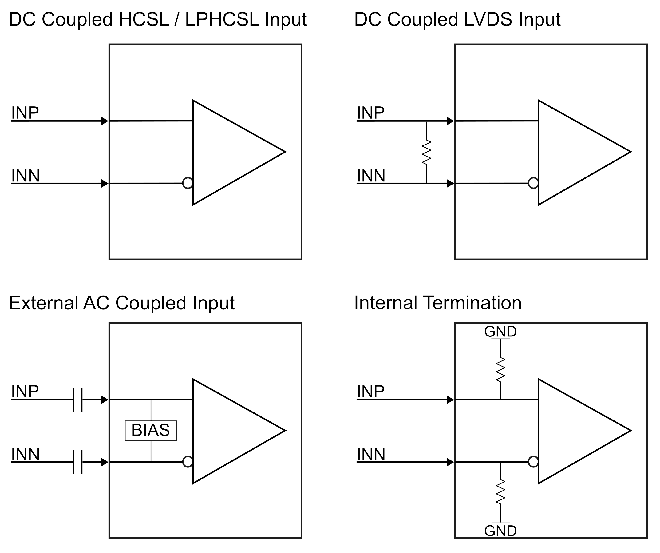
LMKDB1204 can support different input interfaces for either CLKIN depending on the input swing and common mode voltage. There are four input interfaces type that can be configured on LMKDB1204 using external components and internal termination schemes as shown in Figure 4-1. If using a signal generator, then make sure to populate R12 and/or R23 with a 100Ω resistor or use internal / external 50Ω termination to ground.
- DC Coupled HCSL / LP HCSL Input.
- DC Coupled LVDS Input.
- External AC Coupled Input.
- Internal 50Ω to ground terminations.
 Figure 3-1 Input Interfaces
Table 4-8 outlines how to setup all different interfaces supported by LMKDB1204.
Table 3-8 Input Interfaces
| Input Interface | Configuration |
|---|---|
| DC coupled HCSL / LPHCSL (default) | This is the default for the EVM for both clock inputs. R10, R13 and/or R20, R24 values are 0Ω and Input Interface Type on Input page is selected to DC Coupled for each input. |
| DC coupled LVDS input | Populate R12 and/or R23 with a 100Ω resistor and set Input Interface Type on Input page to DC Coupled for each DC coupled LVDS input. |
| External AC coupled input | Replace R10, R13 and/or R20, R24 with 0.1uF capacitor and set Input Interface Type on Input page to AC Coupled for each external AC coupled input. |
| Internal termination | To enable internal 50Ω to ground terminations. Set the Input Termination on Input page to Enabled. |