SNIS169F March   2013  – May 2024 LMT86

PRODUCTION DATA  

  1.   1
  2. Features
  3. Applications
  4. Description
  5. Device Comparison
  6. Pin Configuration and Functions
  7. Specifications
    1. 6.1 Absolute Maximum Ratings
    2. 6.2 ESD Ratings
    3. 6.3 Recommended Operating Conditions
    4. 6.4 Thermal Information
    5. 6.5 Accuracy Characteristics
    6. 6.6 Electrical Characteristics
    7. 6.7 Typical Characteristics
  8. Detailed Description
    1. 7.1 Overview
    2. 7.2 Functional Block Diagram
    3. 7.3 Feature Description
      1. 7.3.1 LMT86 Transfer Function
    4. 7.4 Device Functional Modes
      1. 7.4.1 Mounting and Thermal Conductivity
      2. 7.4.2 Output Noise Considerations
      3. 7.4.3 Capacitive Loads
      4. 7.4.4 Output Voltage Shift
  9. Application and Implementation
    1. 8.1 Application Information
    2. 8.2 Typical Applications
      1. 8.2.1 Connection to an ADC
        1. 8.2.1.1 Design Requirements
        2. 8.2.1.2 Detailed Design Procedure
        3. 8.2.1.3 Application Curve
      2. 8.2.2 Conserving Power Dissipation With Shutdown
        1. 8.2.2.1 Design Requirements
        2. 8.2.2.2 Detailed Design Procedure
        3. 8.2.2.3 Application Curves
  10. Power Supply Recommendations
  11. 10Layout
    1. 10.1 Layout Guidelines
    2. 10.2 Layout Example
  12. 11Device and Documentation Support
    1. 11.1 Receiving Notification of Documentation Updates
    2. 11.2 Support Resources
    3. 11.3 Trademarks
    4. 11.4 Electrostatic Discharge Caution
    5. 11.5 Glossary
  13. 12Revision History
  14. 13Mechanical, Packaging, and Orderable Information

Application Curves

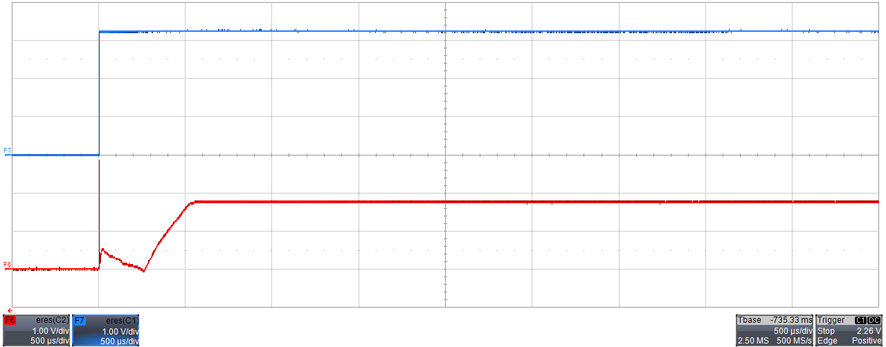
LMT86 Output Turnon Response Time Without a Capacitive Load and VDD =
                        3.3 V
Time: 500 µs/div; Top Trace: VDD 1 V/div; Bottom Trace: OUT 1 V/div
Figure 8-4 Output Turnon Response Time Without a Capacitive Load and VDD = 3.3 V
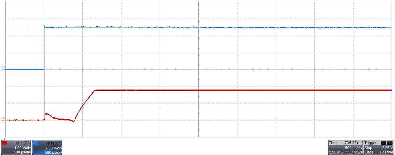
LMT86 Output Turnon Response Time Without a Capacitive Load and VDD =
                        5 V
Time: 500 µs/div; Top Trace: VDD 2 V/div; Bottom Trace: OUT 1 V/div
Figure 8-6 Output Turnon Response Time Without a Capacitive Load and VDD = 5 V
LMT86 Output Turnon Response Time With a 1.1-nF Capacitive Load and
                            VDD = 3.3 V
Time: 500 µs/div; Top Trace: VDD 1 V/div; Bottom Trace: OUT 1 V/div
Figure 8-5 Output Turnon Response Time With a 1.1-nF Capacitive Load and VDD = 3.3 V
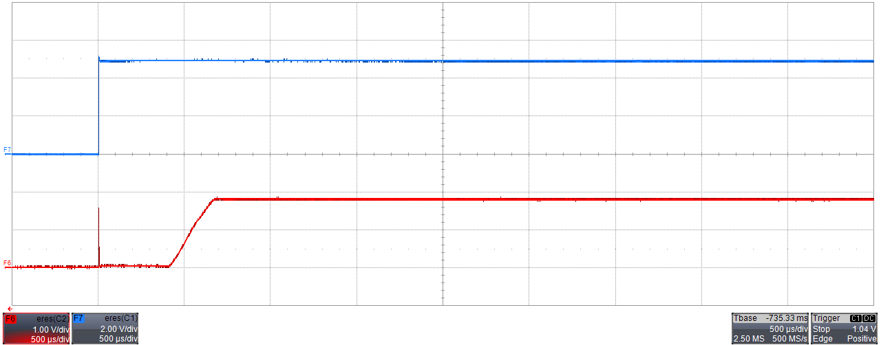
LMT86 Output Turnon Response Time With 1.1-nF Capacitive Load and VDD = 5 V
Time: 500 µs/div; Top Trace: VDD 2 V/div; Bottom Trace: OUT 1 V/div
Figure 8-7 Output Turnon Response Time With 1.1-nF Capacitive Load and VDD = 5 V