SNIS189D June   2015  – June 2018 LMT01

PRODUCTION DATA.  

  1. Features
  2. Applications
    1.     LMT01 Accuracy
  3. Description
    1.     2-Pin IC Temperature Sensor
  4. Revision History
  5. Pin Configuration and Functions
    1.     Pin Functions
  6. Specifications
    1. 6.1  Absolute Maximum Ratings
    2. 6.2  ESD Ratings
    3. 6.3  Recommended Operating Conditions
    4. 6.4  Thermal Information
    5. 6.5  Electrical Characteristics
    6. 6.6  Electrical Characteristics - TO-92/LPG Pulse Count to Temperature LUT
    7. 6.7  Electrical Characteristics - WSON/DQX Pulse Count to Temperature LUT
    8. 6.8  Switching Characteristics
    9. 6.9  Timing Diagram
    10. 6.10 Typical Characteristics
  7. Detailed Description
    1. 7.1 Overview
    2. 7.2 Functional Block Diagram
    3. 7.3 Feature Description
      1. 7.3.1 Output Interface
      2. 7.3.2 Output Transfer Function
      3. 7.3.3 Current Output Conversion to Voltage
    4. 7.4 Device Functional Modes
  8. Application and Implementation
    1. 8.1 Application Information
      1. 8.1.1 Mounting, Temperature Conductivity, and Self-Heating
    2. 8.2 Typical Application
      1. 8.2.1 3.3-V System VDD MSP430 Interface - Using Comparator Input
        1. 8.2.1.1 Design Requirements
        2. 8.2.1.2 Detailed Design Procedure
          1. 8.2.1.2.1 Setting the MSP430 Threshold and Hysteresis
        3. 8.2.1.3 Application Curves
    3. 8.3 System Examples
  9. Power Supply Recommendations
  10. 10Layout
    1. 10.1 Layout Guidelines
    2. 10.2 Layout Example
  11. 11Device and Documentation Support
    1. 11.1 Receiving Notification of Documentation Updates
    2. 11.2 Community Resources
    3. 11.3 Trademarks
    4. 11.4 Electrostatic Discharge Caution
    5. 11.5 Glossary
  12. 12Mechanical, Packaging, and Orderable Information

Pin Configuration and Functions

DQX Package
2-Pin WSON
Bottom View
LMT01 PinOut_DFN_SNIS189.gif
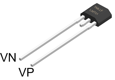
LPG Package
2-Pin TO-92
Top View
LMT01 pin-name-01-pkg-SNIS189.gif

Pin Functions

PIN TYPE DESCRIPTION
NAME TO-92S WSON
VP 2 1 Input Positive voltage pin; may be connected to system power supply or bias resistor.
VN 1 2 Output Negative voltage pin; may be connected to system ground or a bias resistor.