SNIS189D June 2015 – June 2018 LMT01
PRODUCTION DATA.
- 1 Features
- 2 Applications
- 3 Description
- 4 Revision History
- 5 Pin Configuration and Functions
-
6 Specifications
- 6.1 Absolute Maximum Ratings
- 6.2 ESD Ratings
- 6.3 Recommended Operating Conditions
- 6.4 Thermal Information
- 6.5 Electrical Characteristics
- 6.6 Electrical Characteristics - TO-92/LPG Pulse Count to Temperature LUT
- 6.7 Electrical Characteristics - WSON/DQX Pulse Count to Temperature LUT
- 6.8 Switching Characteristics
- 6.9 Timing Diagram
- 6.10 Typical Characteristics
- 7 Detailed Description
- 8 Application and Implementation
- 9 Power Supply Recommendations
- 10Layout
- 11Device and Documentation Support
- 12Mechanical, Packaging, and Orderable Information
9 Power Supply Recommendations
Because the LMT01 is only a 2-pin device the power pins are common with the signal pins, thus the LMT01 has a floating supply that can vary greatly. The LMT01 has an internal regulator that provides a stable voltage to internal circuitry.
Take care to prevent reverse biasing of the LMT01 as exceeding the absolute maximum ratings may cause damage to the device.
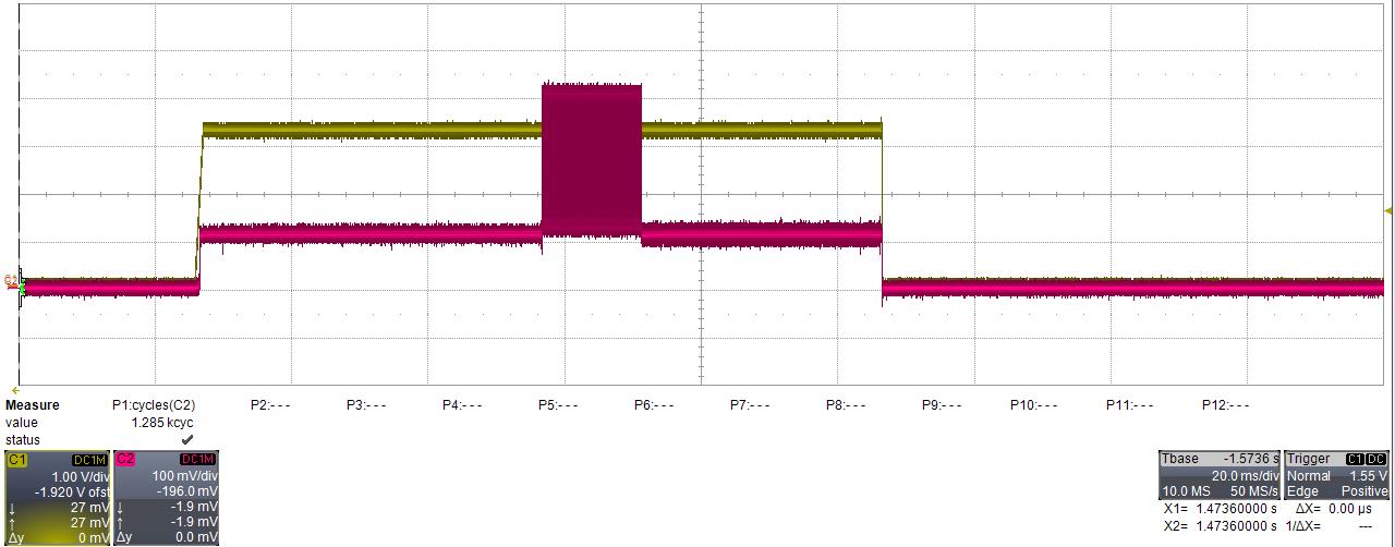
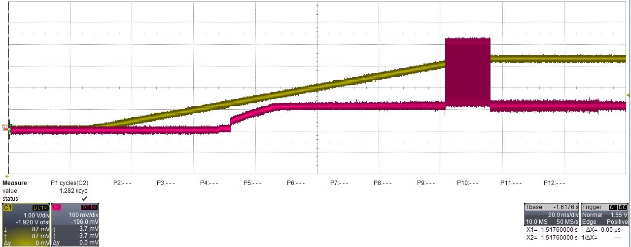
Power supply ramp rate can effect the accuracy of the first result transmitted by the LMT01. As shown in Figure 36 with a 1-ms rise time, the LMT01 output code is at 1286, which converts to 30.125°C. The scope photo shown in Figure 37 reflects what happens when the rise time is too slow. In Figure 37, the power supply (yellow trace) is still ramping up to final value while the LMT01 (red trace) has already started a conversion. This causes the output pulse count to decrease from the previously shown 1286, to 1282 (or 29.875°C). Thus, for slow ramp rates, TI recommends that the first conversion be discarded. For even slower ramp rates, more than one conversion may have to be discarded as TI recommends that either the power supply be within final value before a conversion is used or that ramp rates be faster than 2.5 ms.

| Yellow trace = 1 V/div, Red trace = 100 mV/div, Time Base = 20 ms/div | ||
| TA= 30°C | LMT01 Pulse Count = 1286 | |
| VP-VN = 3.3 V | Rise Time = 1 ms | |

| Yellow trace = 1V/div, Red trace = 100 mV/div, Time base = 20 ms/div | ||
| TA=30°C | LMT01 Pulse Count = 1282 | |
| VP-VN=3.3 V | Rise Time = 100 ms | |