SNIS232A October   2023  – June 2024 ISOTMP35

PRODUCTION DATA  

  1.   1
  2. Features
  3. Applications
  4. Description
  5. Pin Configuration and Functions
  6. Specifications
    1. 5.1  Absolute Maximum Ratings
    2. 5.2  ESD Ratings
    3. 5.3  Recommended Operating Conditions
    4. 5.4  Thermal Information
    5. 5.5  Insulation Specification
    6. 5.6  Power Ratings
    7. 5.7  Safety-Related Certifications
    8. 5.8  Safety Limiting Values
    9. 5.9  Electrical Characteristics
    10. 5.10 Typical Characteristics
  7. Detailed Description
    1. 6.1 Overview
    2. 6.2 Functional Block Diagram
    3. 6.3 Features Description
      1. 6.3.1 Integrated Isolation Barrier and Thermal Response
      2. 6.3.2 Analog Output
        1. 6.3.2.1 Output Accuracy
        2. 6.3.2.2 Output Voltage Linearity
        3. 6.3.2.3 Drive Capability
        4. 6.3.2.4 Common Mode Transient Immunity (CMTI)
      3. 6.3.3 Thermal Response
    4. 6.4 Device Functional Modes
  8. Application and Implementation
    1. 7.1 Application Information
      1. 7.1.1 Output Voltage Linearity
      2. 7.1.2 Load Regulation
      3. 7.1.3 Start-Up Settling Time
      4. 7.1.4 Thermal Response
      5. 7.1.5 External Buffer
      6. 7.1.6 ADC Selection and Impact on Accuracy
      7. 7.1.7 Implementation Guidelines
      8. 7.1.8 PSRR
    2. 7.2 Typical Application
      1. 7.2.1 Design Requirements
      2. 7.2.2 Detailed Design Procedure
        1. 7.2.2.1 Insulation Lifetime
    3. 7.3 Power Supply Recommendations
    4. 7.4 Layout
      1. 7.4.1 Layout Guidelines
      2. 7.4.2 Layout Example
  9. Device and Documentation Support
    1. 8.1 Documentation Support
      1. 8.1.1 Related Documentation
    2. 8.2 Receiving Notification of Documentation Updates
    3. 8.3 Support Resources
    4. 8.4 Trademarks
    5. 8.5 Electrostatic Discharge Caution
    6. 8.6 Glossary
  10. Revision History
  11. 10Mechanical, Packaging, and Orderable Information

Typical Characteristics

at TA = 25°C (unless otherwise noted)
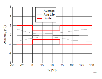
ISOTMP35 Accuracy vs TA Temperature
VDD = 2.3 to 5.5V, IOUT = 0µA, CLOAD = 1000pF
Figure 5-1 Accuracy vs TA Temperature
ISOTMP35 Changes in Accuracy vs Ambient Temperature (Due to Load)
IOUT = from 0µA to 100µA, CLOAD = 1000pF
Figure 5-3 Changes in Accuracy vs Ambient Temperature (Due to Load)
ISOTMP35 Load Regulation vs Ambient Temperature
VDD = 2.3V, CLOAD = 1000pF
Figure 5-5 Load Regulation vs Ambient Temperature
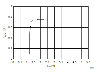
ISOTMP35 Output Voltage vs Power Supply
TA = 25°C
Figure 5-7 Output Voltage vs Power Supply
ISOTMP35 Output vs. Settling Time to Ramp VDD
TA = 25°C, VDD Ramp Rate = 5V/ms
Figure 5-9 Output vs. Settling Time to Ramp VDD
ISOTMP35 Output Impedance vs Frequency
TA = 25°C, VDD = 5V, IOUT = 100µA
Figure 5-11 Output Impedance vs Frequency
ISOTMP35 Output Noise Density
TA = 25°C
Figure 5-13 Output Noise Density
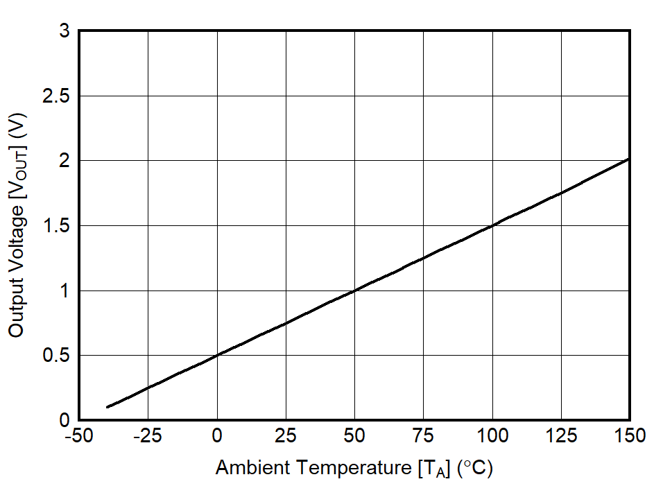
ISOTMP35 Output Voltage vs Ambient Temperature
IOUT = 0µA, CLOAD = 1000pF
Figure 5-2 Output Voltage vs Ambient Temperature
ISOTMP35 Supply Current vs Temperature
IOUT = 0µA, CLOAD = 1000pF
Figure 5-4 Supply Current vs Temperature
ISOTMP35 Line Regulation (Δ°C / ΔVDD) vs Ambient Temperature
VDD = 2.3 to 5.5V, IOUT = 0µA, CLOAD = 1000pF
Figure 5-6 Line Regulation (Δ°C / ΔVDD) vs Ambient Temperature
ISOTMP35 Output vs. Settling Time to Step VDD
TA = 25°C
Figure 5-8 Output vs. Settling Time to Step VDD
ISOTMP35 Thermal Response (Air-to-Fluid Bath)
0.5 × 0.5 inch PCB, Air 25°C to Fluid Bath 150°C
Figure 5-10 Thermal Response (Air-to-Fluid Bath)
ISOTMP35 PSRR vs Frequency
TA = 25°C
Figure 5-12 PSRR vs Frequency