SNLA353 August 2020 DS90LV011A
3 Devices Without Termination Resistors
- Verify in your data sheet whether the receiver that you are using for your design contains an internal termination resistor. The formulas used are similar to obtain values with small differences taking the termination resistor into consideration.
- If your device does not contain internal
termination then the equations shown in Figure 3-1 will be used.
 Figure 3-1 Equations for a Receiver Without
Internal Termination
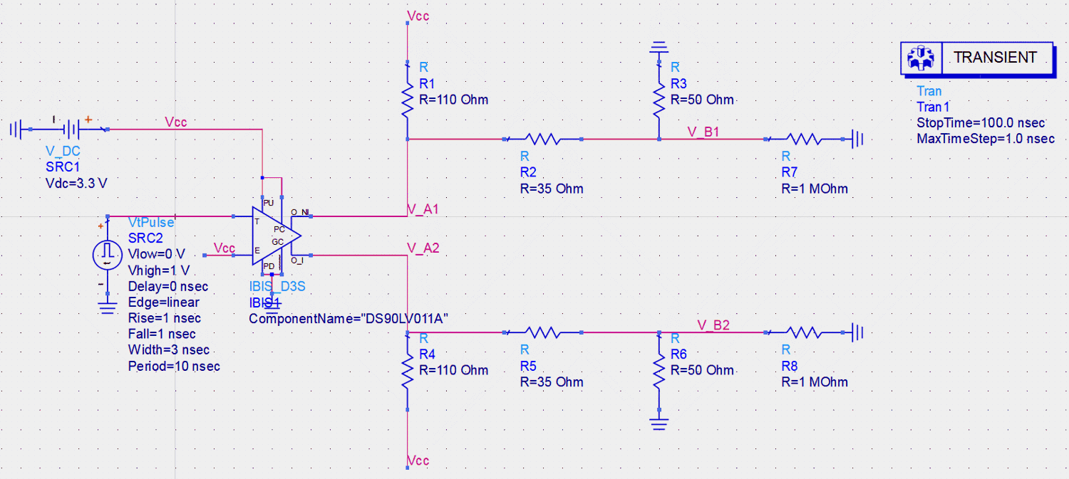
- For the simulation, the following values
will be used:
- VCC = 3.3 V
- VA = 1.2 V, LVDS driver output fixed common mode voltage
- VB = 0.9 V, Sub-LVDS driver output fixed common mode voltage
- RE = 50Ω
- Using the formulas a, b, and c from Section 2, create a system of
equations in order to solve for the resistance values that will best fit the desired
parameters for Sub-LVDS. The following values were obtained from the system of equations:
- R1 = 110Ω
- R2 = 35Ω
- R3 = 50Ω
Now proceed to simulate the circuit in order to verify the behavior.
 Figure 3-2 Schematic for Receivers Without Internal
Termination
Figure 3-2 Schematic for Receivers Without Internal
TerminationNote: R7 and R8 are used to
imitate the high impedance inputs of a receiver.
- The simulation shown in Figure 3-3 demonstrates a voltage swing of approximately:
- VID ≈ 185 mV
- VOD ≈ 320 mV
- VID falls within the desired
range. If the formulas are used to obtain values for VID, VCMF, and
RE with the resistor values and the measured values for VOD &
VA, then the following results can be obtained:
- VID = 188 mV
- VB = 0.85 V
- RE = 48Ω
 Figure 3-3 Simulation Results for Devices Without
Internal Termination