SNLA353 August 2020 DS90LV011A
2 Simulation Setup
The simulations will be done using Keysight ADS with the TI DS90LV011A IBIS model (ds90lv001atmf.ibs) that can be downloaded from the URL: https://www.ti.com/lit/zip/snlm047.
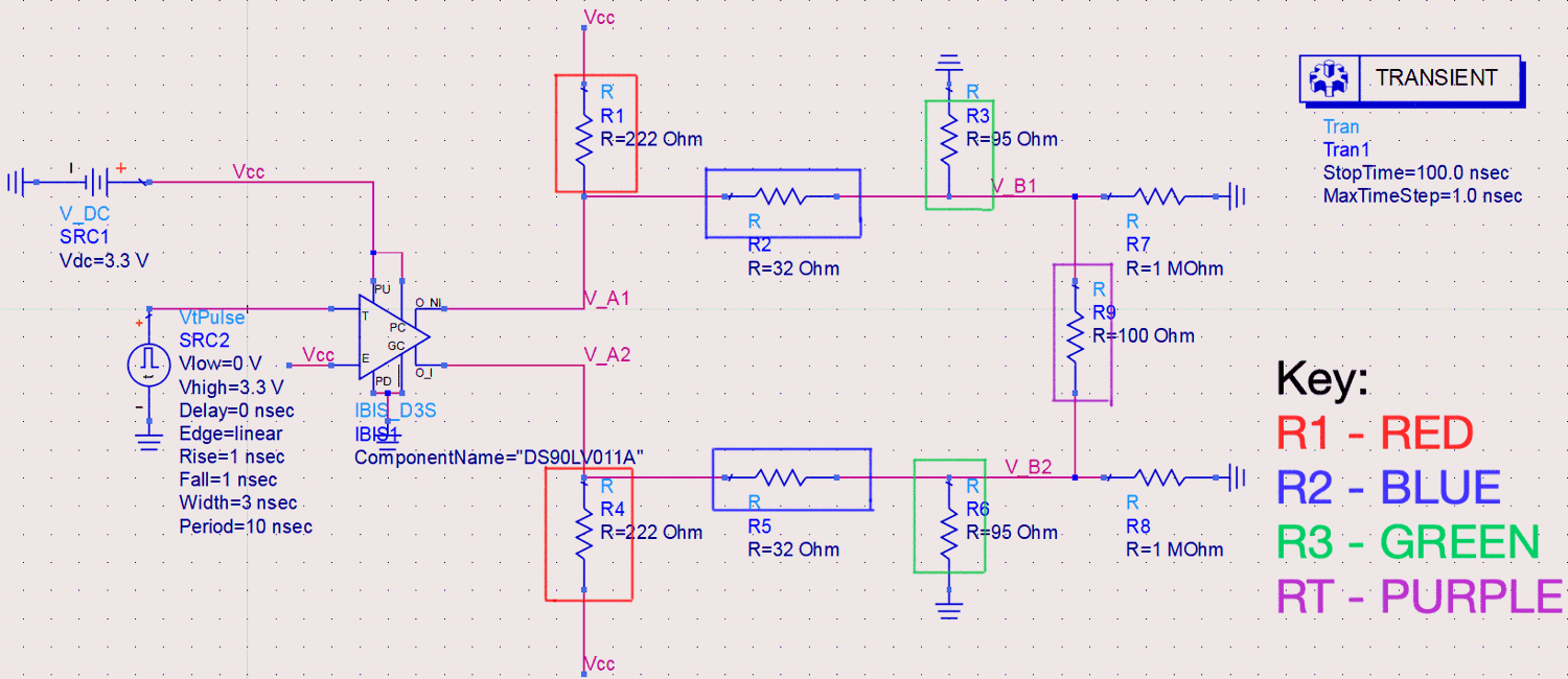
 Figure 2-1 Simulation Block Diagram
 Figure 2-2 Schematic Breakdown
- R1, R2, & R3 make up the resistor network that needs to be created to interface between LVDS and Sub-LVDS. Each differential pair will be made up of these three resistors.
- RT is the value of the termination resistor for devices that contain internal termination (100Ω will be used for this simulation).
- RE is the equivalent
resistance of all the resistors in the resistor networkNote: The Thevenin resistance of these resistors must be approximately 50Ω if the device does or does not contain internal termination; this ensures that the circuit will have a 100Ω equivalent termination resistance between the transmitter and receiver for both differential pairs. The appropriate formulas for each scenario can be seen in the sections below.
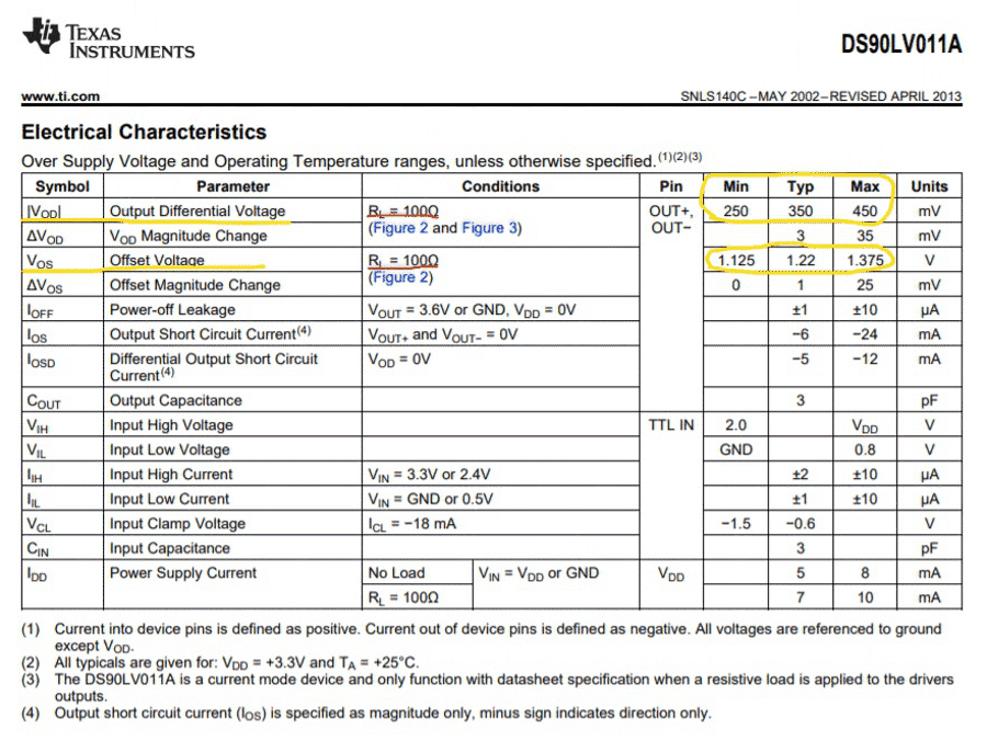
- VA is equivalent to the fixed common mode voltage (VCMF) of the LVDS driver output (1.2 V will be used for this simulation).
- VOD is the output
differential voltage from the LVDS driver.
- The values used can be obtained from the “Electrical Characteristics” section of the data sheet for your specific device.
- For more information, see the DS90LV011A 3V LVDS Single High Speed Differential Driver Data Sheet.
 Figure 2-3 DS90LV011A Data Sheet Electrical
Characteristics
Figure 2-3 DS90LV011A Data Sheet Electrical
Characteristics- VB is equivalent to the fixed common mode voltage (VCMF) of typical Sub-LVDS driver outputs (0.9V will be used for this simulation).
- VID is the output differential voltage of a Sub-LVDS driver. The goal of the simulation is to obtain a value in the operating range for Sub-LVDS transmitters.
Table 2-1 SubLVDS Driver Electrical
Specifications
| SubLVDS Driver Output Levels | ||||||||
|---|---|---|---|---|---|---|---|---|
| Parameter | Min | Typ | Max | Unit | ||||
| VCMF Fixed Common Mode Voltage | 0.8 | 0.9 | 1 | V | ||||
| VOD Differential Voltage Swing | 100 | 150 | 200 | mV | ||||
Table 2-2 SubLVDS Receiver Electrical
Specifications
| SubLVDS Receiver Input Levels | |||||||||||
|---|---|---|---|---|---|---|---|---|---|---|---|
| Parameter | Min | Typ | Max | Unit | |||||||
| Input Voltage | 0.5 | 0.9 | 1.3 | V | |||||||
| Threshold Voltage | -25 | 25 | mV | ||||||||
| Termination Resistance Value | 80 | 100 | 120 | Ω | |||||||