SNLA356 September 2020 DS90UB941AS-Q1 , DS90UH941AS-Q1
4.4 THS-SKIP Configuration
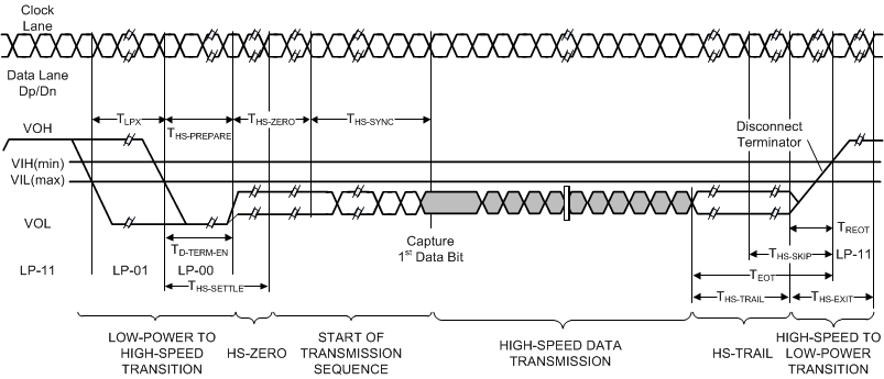
The MIPI D-PHY v1.2 receiver specification requires the sink device to ignore activity on the DSI data lanes at the end of high speed packet transmission prior to re-entering the low power state (LP-11) in order to mask transition effects during the End of Transmission (EoT) sequence. If the THS-SKIP timing parameter is mis-configured, it may result in data errors in the DSI video stream.
 Figure 4-6 High-Speed Data Transmission in
Bursts
Figure 4-6 High-Speed Data Transmission in
BurstsSymptoms:
- Random/intermittent pixel errors
- DSI error flags in the DS90UB941AS-Q1 registers
- Jittering or flickering display
Resolution:
DS90UB941AS-Q1 requires user configuration of the tHS-SKIP timing parameter based on the DSI clock speed applied. The TSKIP_CNT (dec) value is defined in Equation 14, where fDSI is the DSI clock frequency in GHz.
This value must get loaded into DS90UB941AS-Q1 register 0x05[6:1] (in hex) prior to enabling the DSI receiver.
To program TSKIP_CNT, use the following programming steps via I2C:
- Write 0x40 = 0x04 for DSI Port 0 or 0x40 = 0x08 for DSI Port 1
- Write 0x41 = 0x05.
- Write 0x42 = hex(TSKIP_CNT<<1) from Equation 14.
The DS90Ux941AS-Q1 Superframe Design Calculator tool is available in the DS90UB941AS-Q1 product folder, which also includes calculations for TSKIP_CNT.