SNLA431 January 2024 DP83TC812R-Q1 , DP83TC812S-Q1
- 1
- Trademarks
- 1Preface
- Notational Conventions
- 2Related Documentation
- 3Support Resources
-
4Troubleshooting the PHY Application
- 4.1 Schematic and Layout Checklist
- 4.2 Verify Successful Power-up of PHY
- 4.3 Peripheral Pin Checks
- 4.4 Register Dump Comparison
- 4.5 Verifying Strap Configurations
- 4.6 Check the MDI Signal
- 4.7 Link Up Failed Common Issues
- 4.8 Signal Quality Check
- 4.9 Power Up Timing
- 4.10 Loopback Testing
- 4.11 Debugging the MAC Interface
- 4.12 Verify Open Alliance PMA Compliance
- 4.13 Tools and References
- 5Conclusion
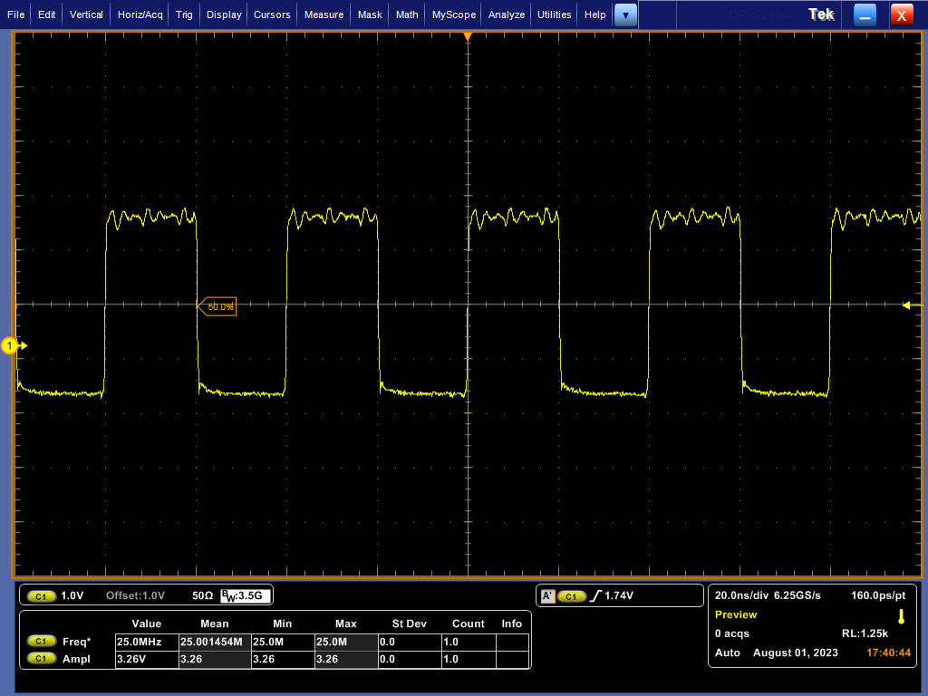
4.3.3 Probe the CLKOUT pin
The reference clock frequency and stability is of utmost importance to maintain proper operation of the PHY. Failure to meet the specifications in the data sheet can lead to bit errors, read/write issues, or total non-operation of the PHY.
Do not probe the crystal directly as this can change the capacitive loading of the circuit and alter the behavior. Instead, probe the CLKOUT pin (pin 16) which is a buffered version of the input reference clock.
Maintain that the frequency is within ±100ppm of the expected value: (40.995 - 50.005Mhz) for RMII slave mode and (24.9975 - 25.0025Mhz) for all other modes.
|
25MHz Crystal Requirements |
||
|---|---|---|
|
Frequency |
25 |
MHz |
|
Max Frequency tolerance and Stability over Temperature and Aging |
±100 |
ppm |
|
Max Equivalent Series Resistance |
100 |
Ω |
 Figure 4-1 DP83TC812 CLK_OUT
Measurements