SNLA443 December 2023 DP83869HM
- 1
- Abstract
- Trademarks
- 1DP83869 Application Overview
- 2Troubleshooting the Application
- 3Operational Mode Clarification
- 4Tools and References
- 5Summary
- 6References
2.6.1 RGMII
Reference the waveforms in this section to verify the expected MAC data and clock signals for RGMII in shift and align modes. To capture data and clock signals, measure close to the receiver end. Note the following requirements for selecting the correct delay mode:
| If MAC's Configuration is: | Required PHY Configuration |
|---|---|
| RGMII Align Mode on TX side | RGMII Shift Mode on TX side |
| RGMII Align Mode on RX side | RGMII Shift Mode on RX side |
| RGMII Shift Mode on TX side | RGMII Align Mode on TX side |
| RGMII Shift Mode on RX side | RGMII Align Mode on RX side |
RX_D[3:0] Data Aligned with RX_CLK
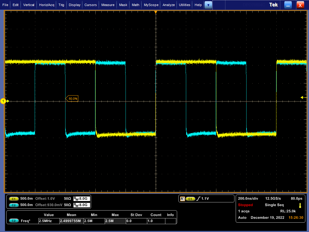
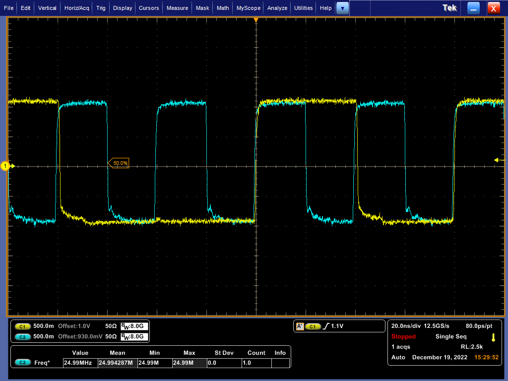
For the PHY set in RX align mode in 10/100Mbps, probe the clock and data signals on the MAC end and compare to the reference waveforms shown below.
 Figure 2-10 10Mbps Data Aligned With
RX_CLK
Figure 2-10 10Mbps Data Aligned With
RX_CLKVerify the frequency of the clock (C2) as 2.5 MHz and the data (C1) being sampled at the rising edge of the clock.
 Figure 2-11 100Mbps Data Aligned With
RX_CLK
Figure 2-11 100Mbps Data Aligned With
RX_CLKVerify the frequency of the clock (C2) as 25 MHz and the data (C1) being sampled at the rising edge of the clock.
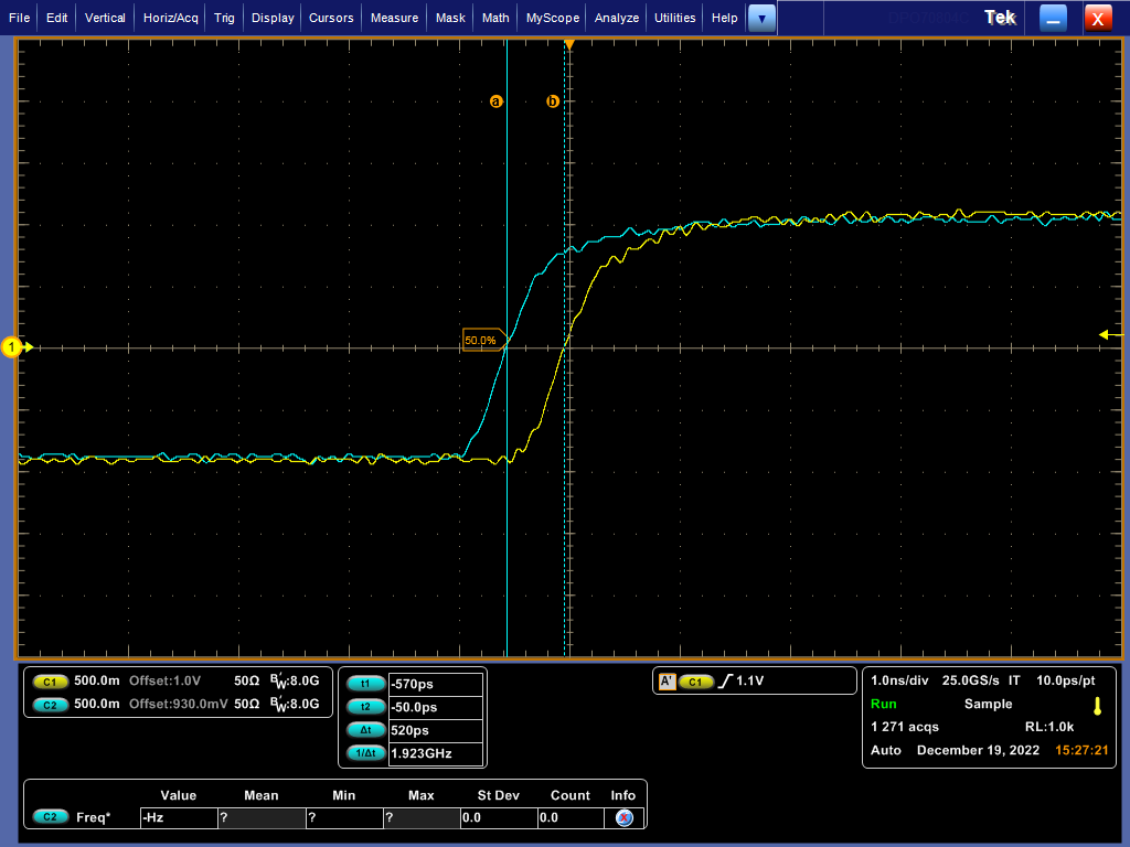
 Figure 2-12 10Mbps Data and Clock Delay in
Align Mode
Figure 2-12 10Mbps Data and Clock Delay in
Align ModeVerify the delay between clock and data is <500ps in align mode.
RX_D[3:0] Data and RX_CLK in Shift Mode
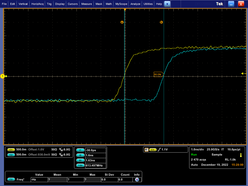
For the PHY set in RX shift mode (0x32) in 10/100Mbps, probe the clock and data signals on the MAC end and compare to the following reference waveforms.
 Figure 2-13 10Mbps Data and RX_CLK in
Shift Mode (4ns Programmed Delay)
Figure 2-13 10Mbps Data and RX_CLK in
Shift Mode (4ns Programmed Delay)Verify the delay between clock and data is >1ns in shift mode. The programmed delay is relative to the clock's initial position in aligned mode. Measuring the difference in the clock's position before and after setting shift mode yields a value closer to the programmed delay.
TX_D[3:0] and TX_CLK in Shift and Align Mode
With the PHY set in TX shift or align mode, probe the data and clock signals on the PHY end and verify the timing requirements below are met:
| PARAMETER | MIN | NOM | MAX | UNIT | |
|---|---|---|---|---|---|
| TskewT | Data to Clock output Skew (at Transmitter) |
–500 | 0 | 500 | ps |
| TskewR | Data to Clock input Skew (at Receiver) |
1 | 1.8 | 2.6 | ns |
| TsetupT | Data to Clock output Setup (at Transmitter – internal delay) |
1.2 | 2 | ns | |
| TholdT | Clock to Data output Hold (at Transmitter – internal delay) |
1.2 | 2 | ns | |
| TsetupR | Data to Clock input Setup (at Reciever – internal delay) |
1 | 2 | ns | |
| TholdR | Clock to Data input Hold (at Receiver – internal delay) |
1 | 2 | ns | |
| Tcyc | Clock Cycle Duration | 7.2 | 8 | 8.8 | ns |
| Duty_G | Duty Cycle for Gigabit | 45 | 50 | 55% | |
| Duty_T | Duty Cycle for 10/100T | 40 | 50 | 60% | |
| TR | Rise Time (20% to 80%) | 0.75 | ns | ||
| TF | Fall Time (20% to 80%) | 0.75 | ns | ||