SNLA475 October 2024 DS250DF410 , DS250DF810 , DS280BR810 , DS280BR820 , DS280DF810 , DS280MB810 , DS560MB410
- 1
- Abstract
- Trademarks
- 1Introduction
- 2Codesign: 25GbE 4-Channel Retimer or Redriver with Crosspoint
- 3Codesign: 25GbE 8-Channel Retimer or Redriver with Crosspoint
- 4Summary
- 5References
3.1 DS250DF810 and DS280DF810 Retimers Overview
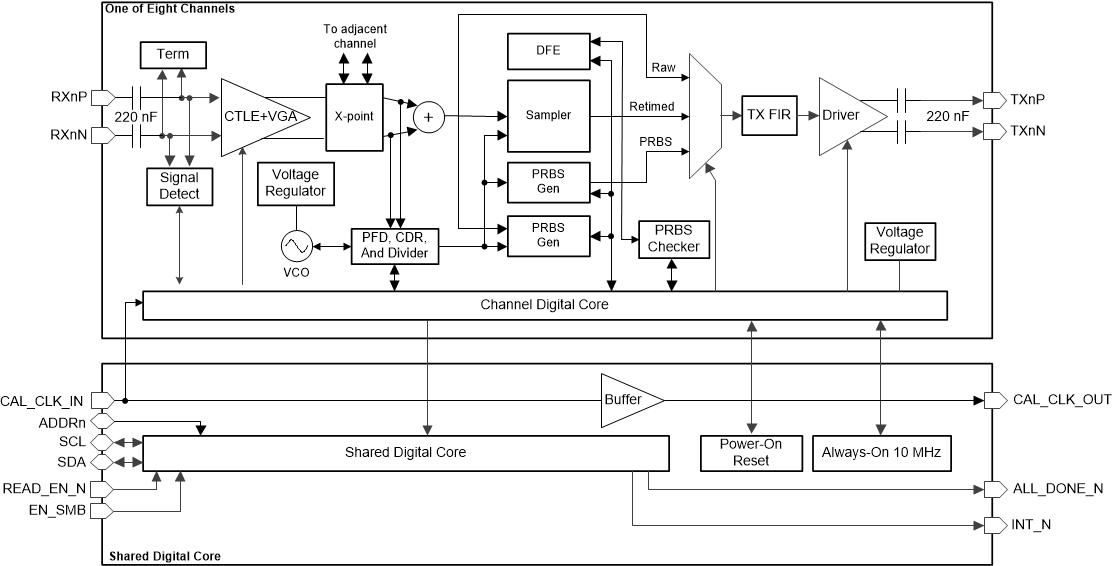
The DS250DF810 and DS280DF810 retimers are both 8 channel retimer devices. The key differentiation between these devices is that DS250DF810 can lock to rates from 20.2752Gbps to 25.8Gbps and supported subrates, while the DS280DF810 can lock to rates from 20.2Gbps to 28.4Gbps and supported subrates. These devices can equalize channels with up to 35dB insertion loss at 12.89GHz using a combination of CTLE and DFE. The DS2x0DF810 also has a 3-tap FIR filter which allows for pre- and post- cursor equalization.
 Figure 3-1 DS2x0DF810 Functional Block
Diagram
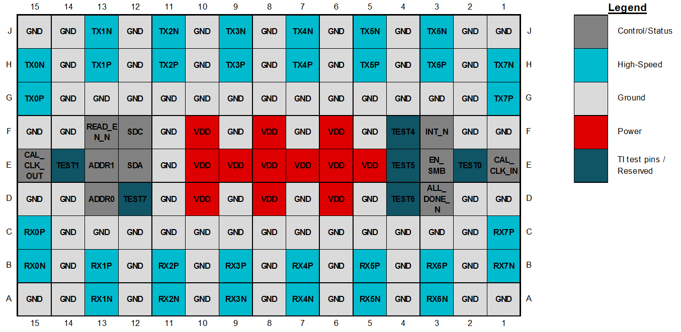
 Figure 3-2 DS2x0DF810 Pin Configuration