SNLS044D May 2000 – July 2016 DS90LV047A
PRODUCTION DATA.
- 1 Features
- 2 Applications
- 3 Description
- 4 Revision History
- 5 Pin Configuration and Functions
- 6 Specifications
- 7 Parameter Measurement Information
- 8 Detailed Description
- 9 Application and Implementation
- 10Power Supply Recommendations
- 11Layout
- 12Device and Documentation Support
- 13Mechanical, Packaging, and Orderable Information
6 Specifications
6.1 Absolute Maximum Ratings
See (1)| MIN | MAX | UNIT | |||
|---|---|---|---|---|---|
| Supply voltage (VCC) | −0.3 | 4 | V | ||
| Input voltage (DIN) | −0.3 | VCC + 0.3 | V | ||
| Enable input voltage (EN, EN*) | −0.3 | VCC + 0.3 | V | ||
| Output voltage (DOUT+, DOUT–) | −0.3 | 3.9 | V | ||
| Short-circuit duration | (DOUT+, DOUT–) | Continuous | |||
| Maximum package power dissipation at +25°C | D0016A package | 1088 | mW | ||
| PW0016A package | 866 | ||||
| Derate D0016A package | above +25°C | 8.5 | mW/°C | ||
| Derate PW0016A package | above +25°C | 6.9 | |||
| Lead temperature | Soldering (4 s) | 260 | °C | ||
| Maximum junction temperature | 150 | °C | |||
| Storage temperature, Tstg | −65 | 150 | °C | ||
(1) Stresses beyond those listed under Absolute Maximum Ratings may cause permanent damage to the device. These are stress ratings only, which do not imply functional operation of the device at these or any other conditions beyond those indicated under Recommended Operating Conditions. Exposure to absolute-maximum-rated conditions for extended periods may affect device reliability.
6.2 ESD Ratings
| VALUE | UNIT | |||
|---|---|---|---|---|
| V(ESD) | Electrostatic discharge(1) | Human-body model (HBM) | ±10000 | V |
| Machine Model | ±1200 | |||
(1) ESD Ratings:
HBM (1.5 kΩ, 100 pF)
EIAJ (0 Ω, 200 pF)
HBM (1.5 kΩ, 100 pF)
EIAJ (0 Ω, 200 pF)
6.3 Recommended Operating Conditions
| MIN | NOM | MAX | UNIT | ||
|---|---|---|---|---|---|
| Supply voltage, VCC | 3 | 3.3 | 3.6 | V | |
| Operating free air temperature, TA | −40 | 25 | 85 | °C | |
6.4 Thermal Information
| THERMAL METRIC(1) | DS90LV047A | UNIT | |
|---|---|---|---|
| PW (TSSOP) | |||
| 16 PINS | |||
| RθJA | Junction-to-ambient thermal resistance | 114 | °C/W |
| RθJC(top) | Junction-to-case (top) thermal resistance | 51 | °C/W |
| RθJB | Junction-to-board thermal resistance | 59 | °C/W |
| ψJT | Junction-to-top characterization parameter | 8 | °C/W |
| ψJB | Junction-to-board characterization parameter | 58 | °C/W |
(1) For more information about traditional and new thermal metrics, see the Semiconductor and IC Package Thermal Metrics application report.
6.5 Electrical Characteristics
Over supply voltage and operating temperature ranges, unless otherwise specified(1)(2)(3)| PARAMETER | TEST CONDITIONS | PIN | MIN | TYP | MAX | UNIT | |
|---|---|---|---|---|---|---|---|
| VOD1 | Differential output voltage | RL = 100 Ω (Figure 17) | DOUT−
DOUT+ |
250 | 310 | 450 | mV |
| ΔVOD1 | Change in magnitude of VOD1 for complementary output states | 1 | 35 | |mV| | |||
| VOS | Offset voltage | 1.125 | 1.17 | 1.375 | V | ||
| ΔVOS | Change in magnitude of VOS for complementary output states | 1 | 25 | |mV| | |||
| VOH | Output high voltage | 1.33 | 1.6 | V | |||
| VOL | Output low voltage | 0.9 | 1.02 | V | |||
| VIH | Input high voltage | DIN, EN, EN* | 2 | VCC | V | ||
| VIL | Input low voltage | GND | 0.8 | V | |||
| IIH | Input high current | VIN = VCC or 2.5 V | −10 | 2 | +10 | µA | |
| IIL | Input low current | VIN = GND or 0.4 V | −10 | −2 | +10 | µA | |
| VCL | Input clamp voltage | ICL = −18 mA | −1.5 | −0.8 | V | ||
| IOS | Output short-circuit current(4) | ENABLED, DIN = VCC, DOUT+ = 0 V or DIN = GND, DOUT− = 0 V |
DOUT−
DOUT+ |
−4.2 | −9 | mA | |
| IOSD | Differential output short-circuit current(4) | ENABLED, VOD = 0 V | −4.2 | −9 | mA | ||
| IOFF | Power-off leakage | VOUT = 0 V or 3.6 V, VCC = 0 V or Open | −20 | ±1 | 20 | µA | |
| IOZ | Output TRI-STATE current | EN = 0.8 V and EN* = 2.0 V VOUT = 0 V or VCC |
−10 | ±1 | 10 | µA | |
| ICC | No load supply current drivers enabled | DIN = VCC or GND | VCC | 4 | 8 | mA | |
| ICCL | Loaded supply current drivers enabled | RL = 100 Ω all channels, DIN = VCC or GND (all inputs) | 20 | 30 | mA | ||
| ICCZ | No load supply current drivers disabled | DIN = VCC or GND, EN = GND, EN* = VCC |
2.2 | 6 | mA | ||
(1) Current into device pins is defined as positive. Current out of device pins is defined as negative. All voltages are referenced to ground except: VOD1 and ΔVOD1.
(2) All typicals are given for: VCC = 3.3 V, TA = +25°C.
(3) The DS90LV047A is a current mode device and only functions within datasheet specifications when a resistive load is applied to the driver outputs typical range is (90 Ω to 110 Ω).
(4) Output short circuit current (IOS) is specified as magnitude only, minus sign indicates direction only.
6.6 Switching Characteristics
VCC = +3.3V ± 10%, TA = −40°C to +85°C(1)(2)(3)| PARAMETER | TEST CONDITIONS | MIN | TYP | MAX | UNIT | |
|---|---|---|---|---|---|---|
| tPHLD | Differential propagation delay high to low | RL = 100 Ω, CL = 15 pF (Figure 18 and Figure 19) |
0.5 | 0.9 | 1.7 | ns |
| tPLHD | Differential propagation delay low to high | 0.5 | 1.2 | 1.7 | ns | |
| tSKD1 | Differential pulse skew |tPHLD − tPLHD|(4) | 0 | 0.3 | 0.4 | ns | |
| tSKD2 | Channel-to-channel skew(5) | 0 | 0.4 | 0.5 | ns | |
| tSKD3 | Differential part-to-part skew(6) | 0 | 1 | ns | ||
| tSKD4 | Differential part-to-part skew(7) | 0 | 1.2 | ns | ||
| tTLH | Rise time | 0.5 | 1.5 | ns | ||
| tTHL | Fall time | 0.5 | 1.5 | ns | ||
| tPHZ | Disable time high to Z | RL = 100 Ω, CL = 15 pF (Figure 20 and Figure 21) |
2 | 5 | ns | |
| tPLZ | Disable time low to Z | 2 | 5 | ns | ||
| tPZH | Enable time Z to high | 3 | 7 | ns | ||
| tPZL | Enable time Z to low | 3 | 7 | ns | ||
| fMAX | Maximum operating frequency(8) | 200 | 250 | MHz | ||
(1) All typicals are given for: VCC = 3.3 V, TA = +25°C.
(2) Generator waveform for all tests unless otherwise specified: f = 1 MHz, ZO = 50 Ω, tr ≤ 1 ns, and tf ≤ 1 ns.
(3) CL includes probe and jig capacitance.
(4) tSKD1 |tPHLD – tPLHD| is the magnitude difference in differential propagation delay time between the positive going edge and the negative going edge of the same channel.
(5) tSKD2 is the differential channel-to-channel skew of any event on the same device.
(6) tSKD3, differential part-to-part skew, is defined as the difference between the minimum and maximum specified differential propagation delays. This specification applies to devices at the same VCC and within 5°C of each other within the operating temperature range.
(7) tSKD4, part to part skew, is the differential channel-to-channel skew of any event between devices. This specification applies to devices over recommended operating temperature and voltage ranges, and across process distribution. tSKD4 is defined as |Max − Min| differential propagation delay.
(8) fMAX generator input conditions: tr = tf < 1 ns (0% to 100%), 50% duty cycle, 0 V to 3 V. Output criteria: duty cycle = 45% / 55%,
VOD > 250 mV, all channels switching.
VOD > 250 mV, all channels switching.
6.7 Typical Characteristics
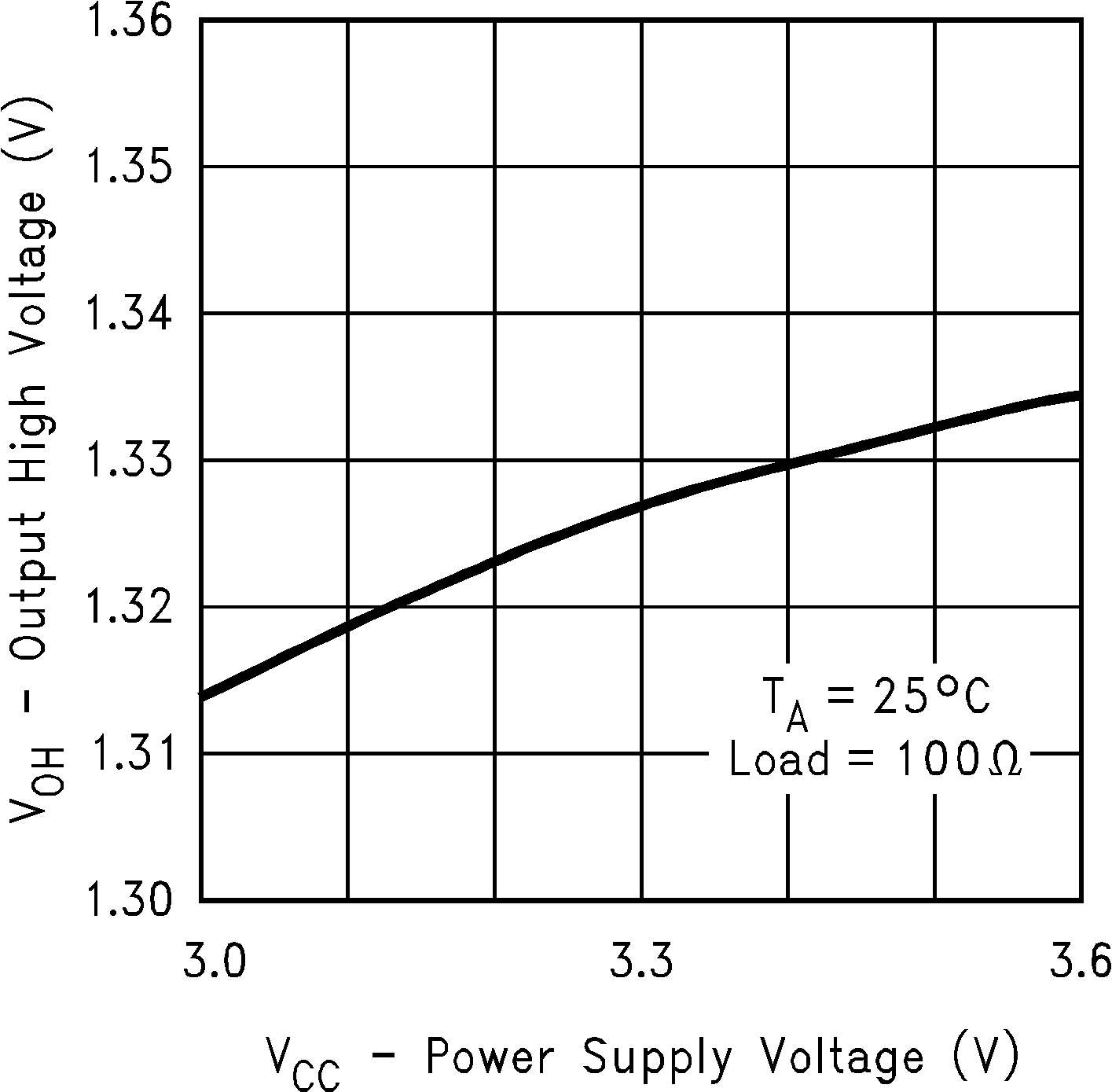 Figure 1. Output High Voltage vs Power Supply Voltage
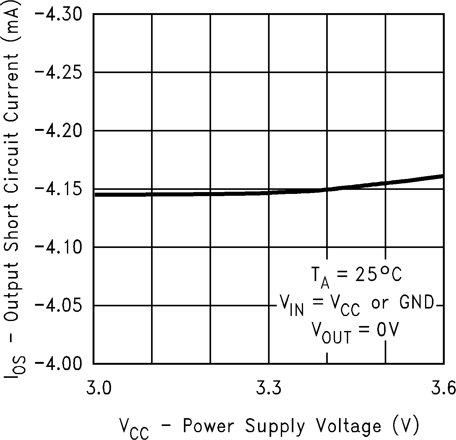 Figure 3. Output Short Circuit Current vs
Power Supply Voltage
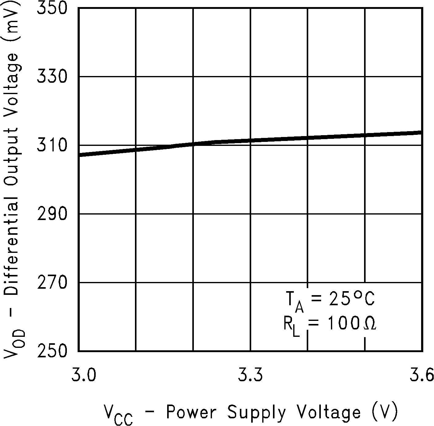 Figure 5. Differential Output Voltage vs
Power Supply Voltage
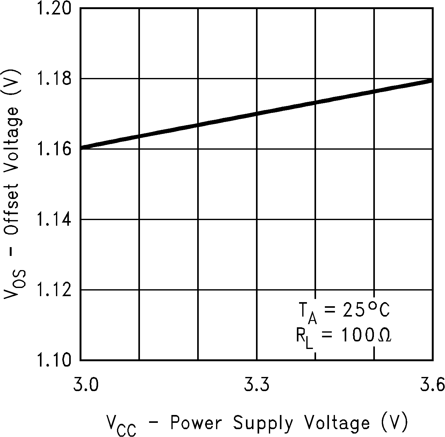 Figure 7. Offset Voltage vs Power Supply Voltage
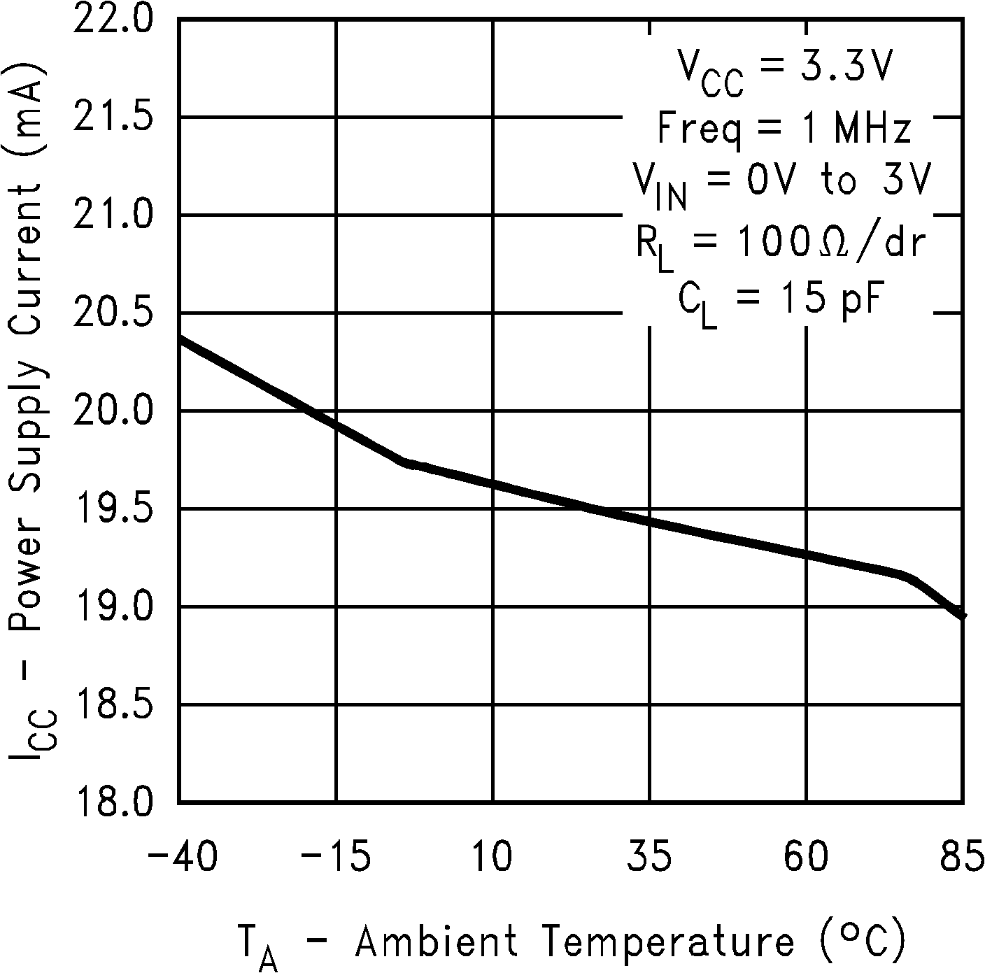 Figure 9. Power Supply Current vs Ambient Temperature
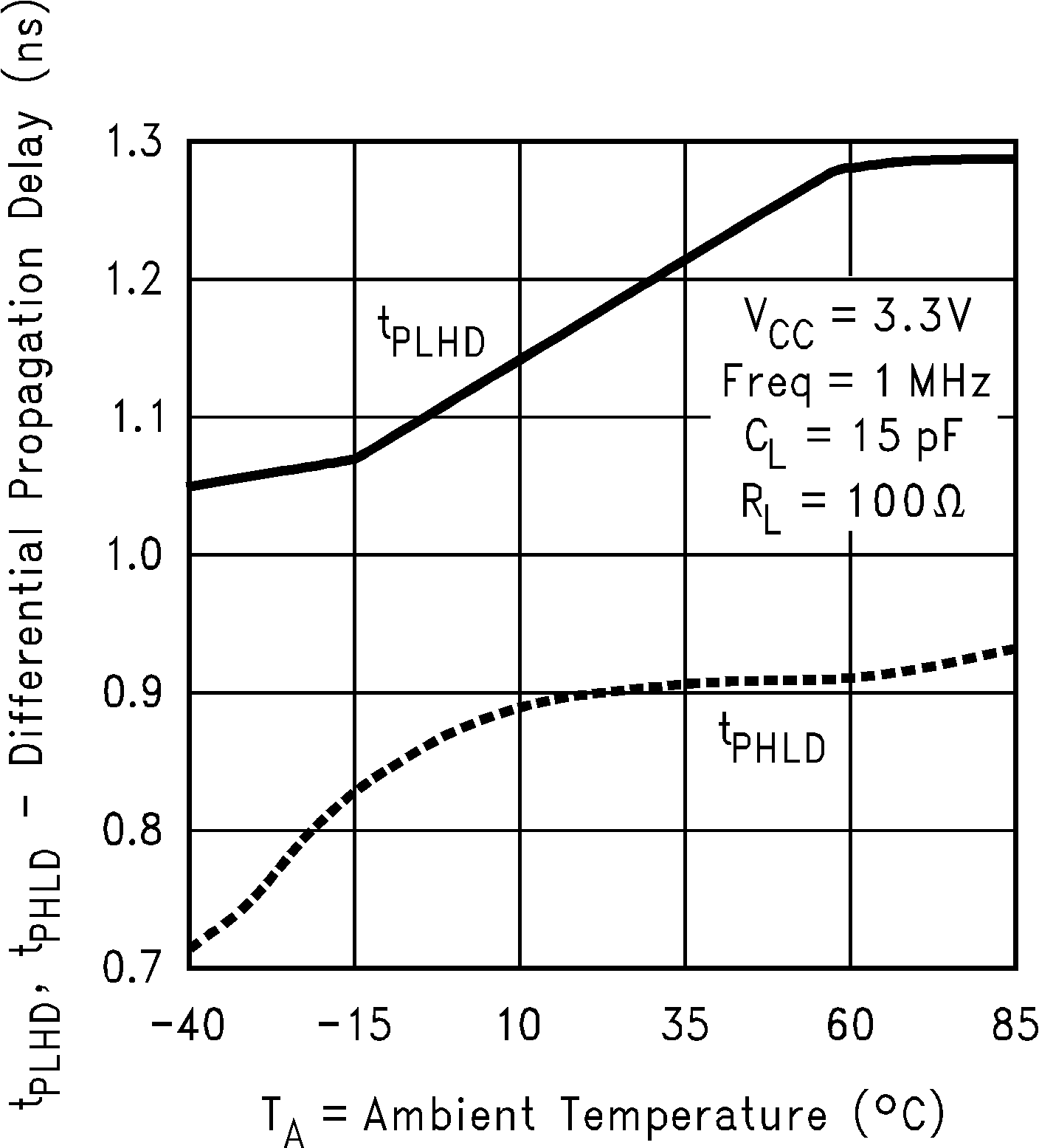 Figure 11. Differential Propagation Delay vs
Ambient Temperature
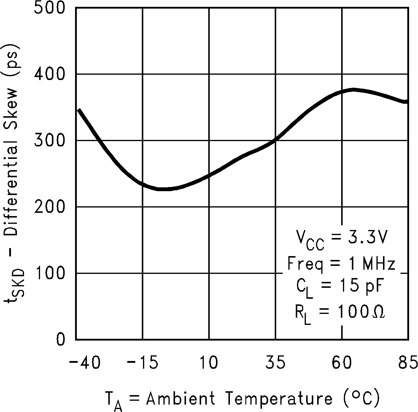 Figure 13. Differential Skew vs Ambient Temperature
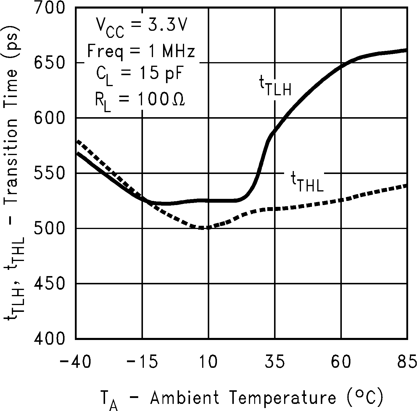 Figure 15. Transition Time vs Ambient Temperature
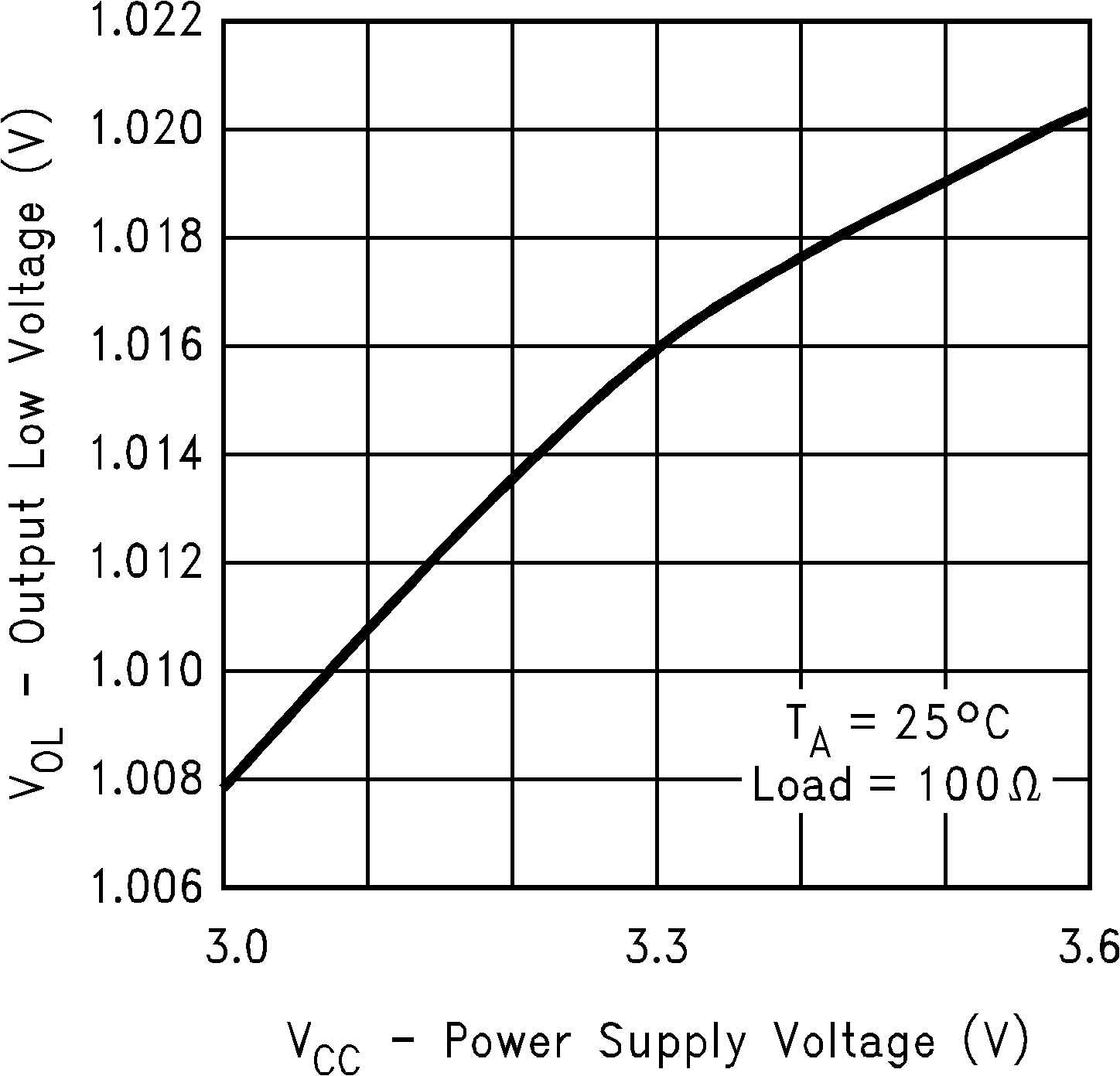 Figure 2. Output Low Voltage vs Power Supply Voltage
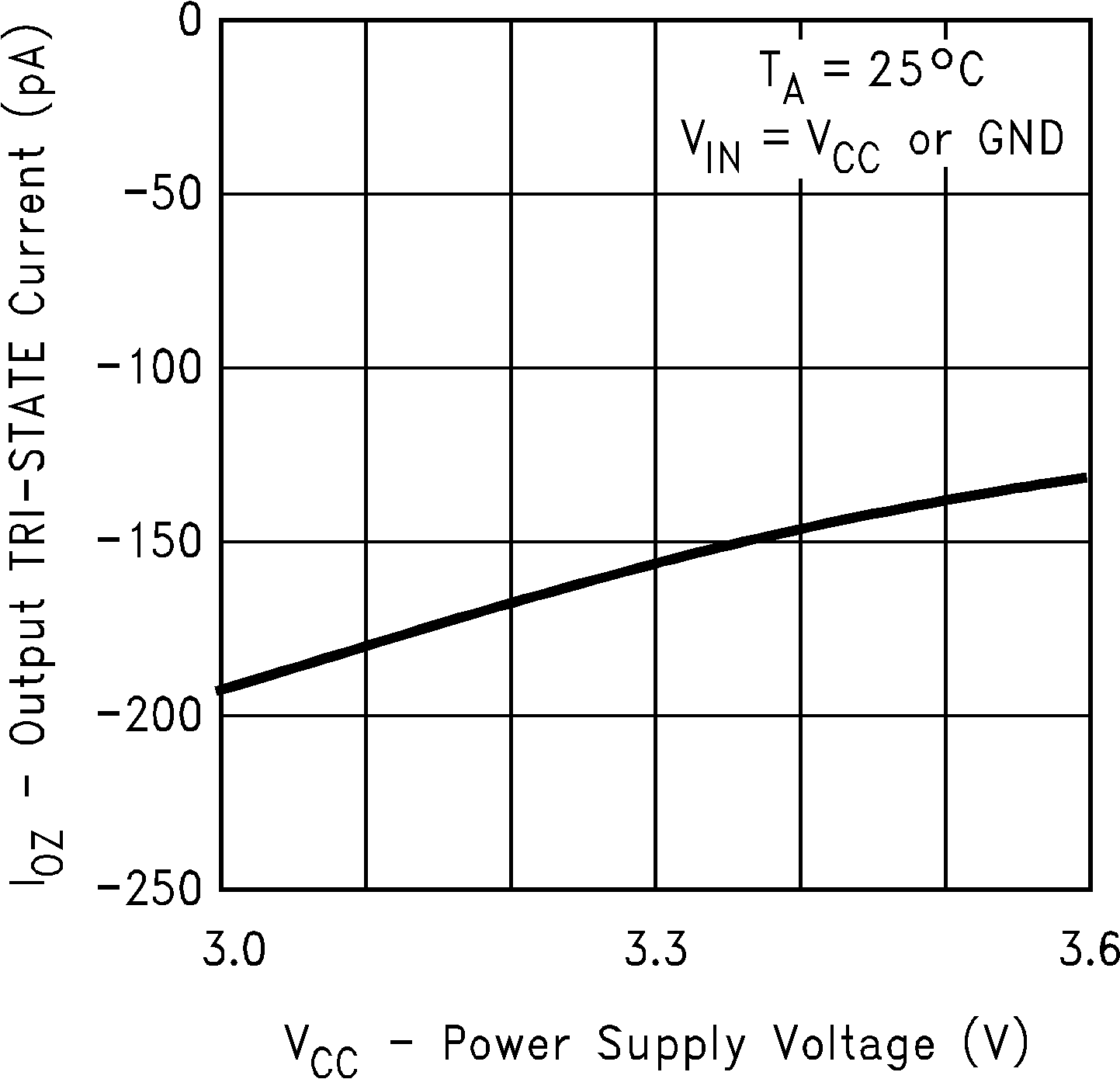 Figure 4. Output TRI-STATE Current vs
Power Supply Voltage
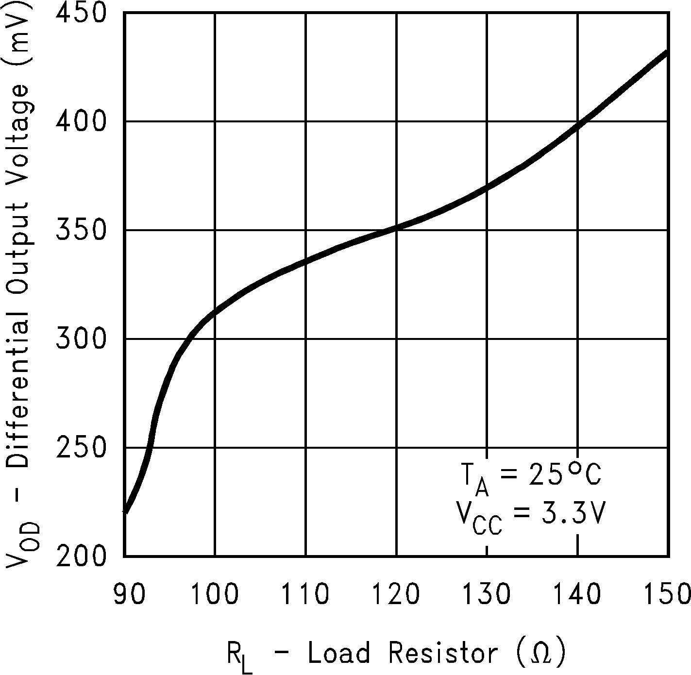 Figure 6. Differential Output Voltage vs Load Resistor
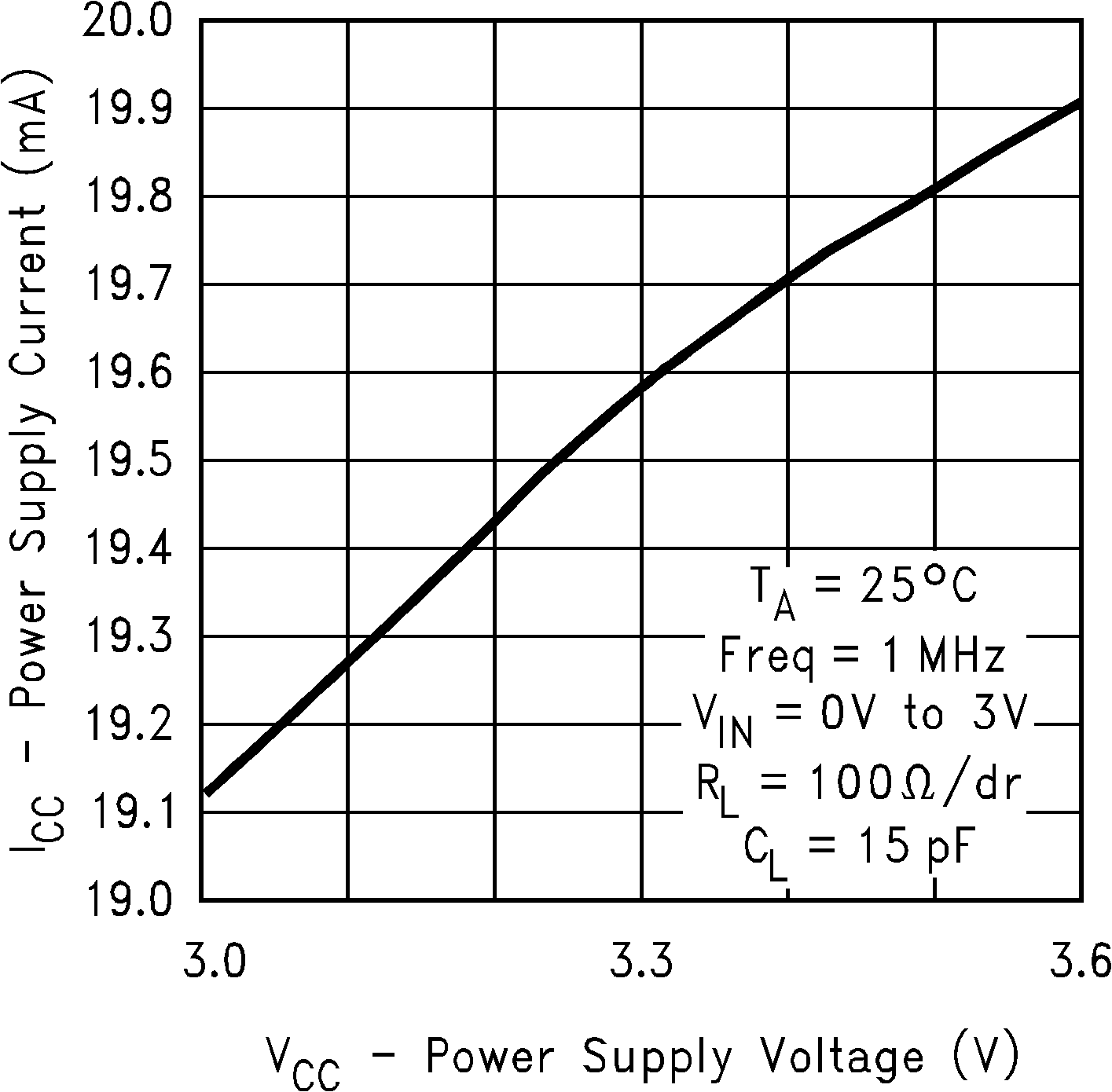 Figure 8. Power Supply Current vs Power Supply Voltage
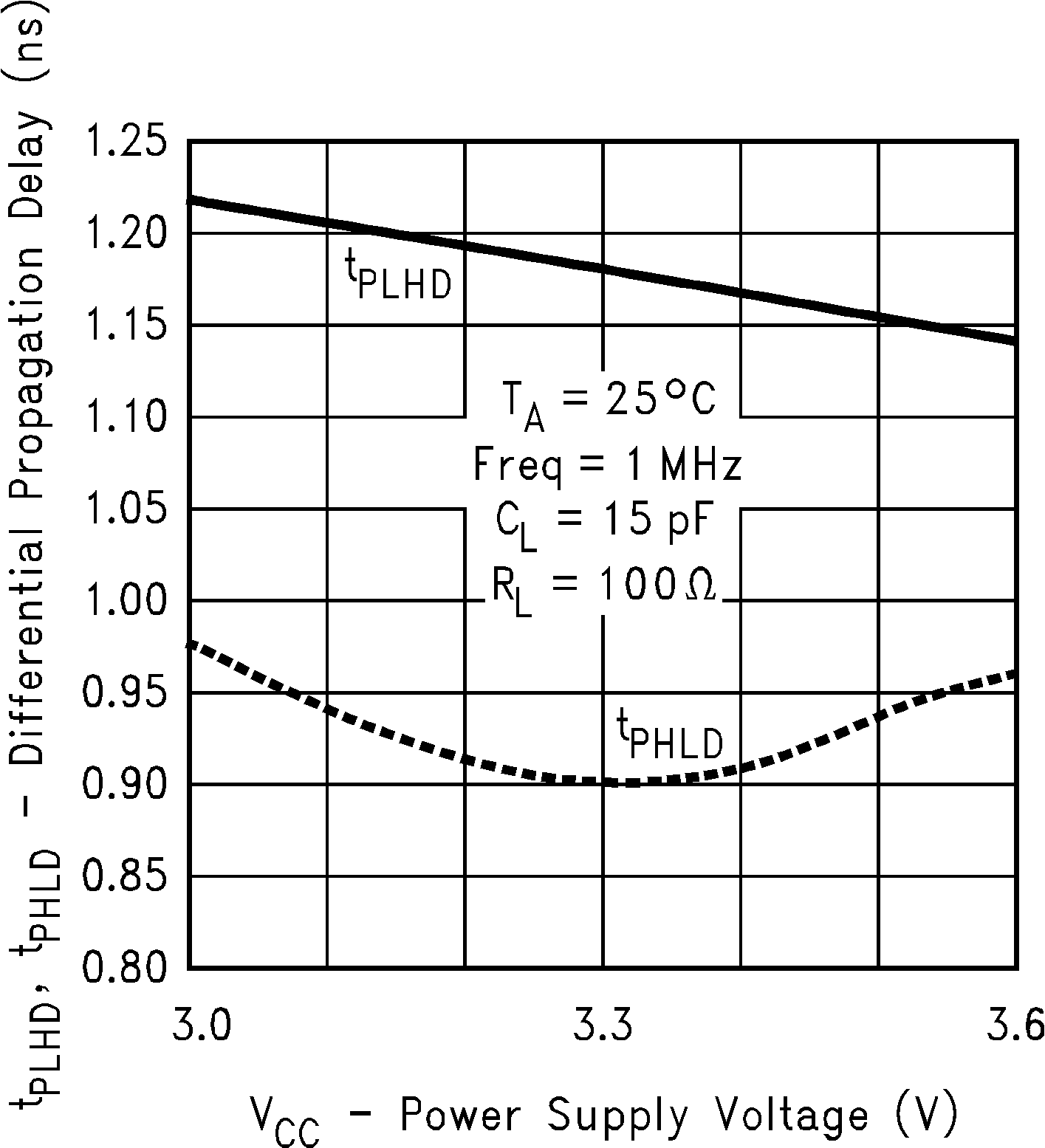 Figure 10. Differential Propagation Delay vs
Power Supply Voltage
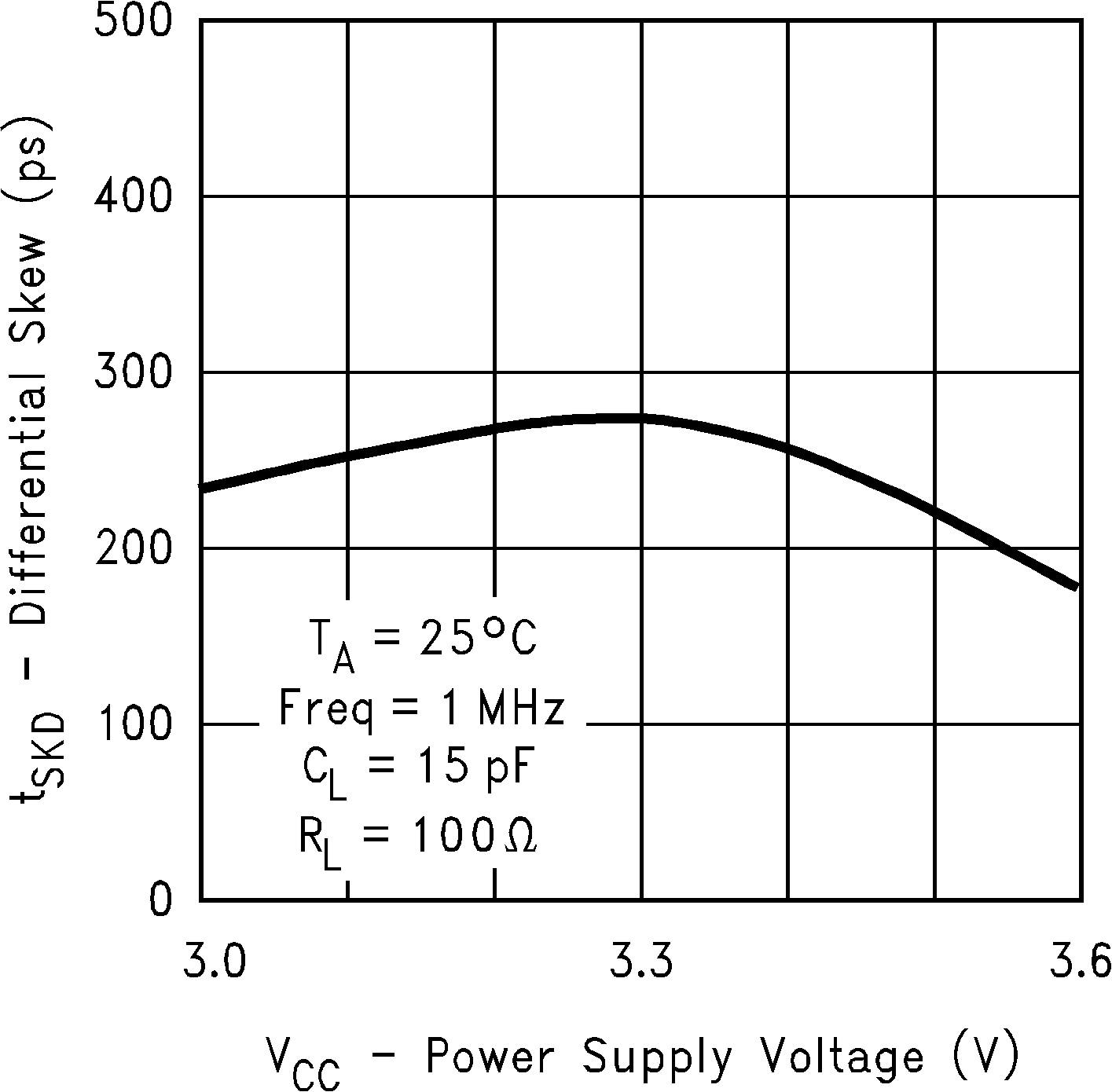 Figure 12. Differential Skew vs Power Supply Voltage
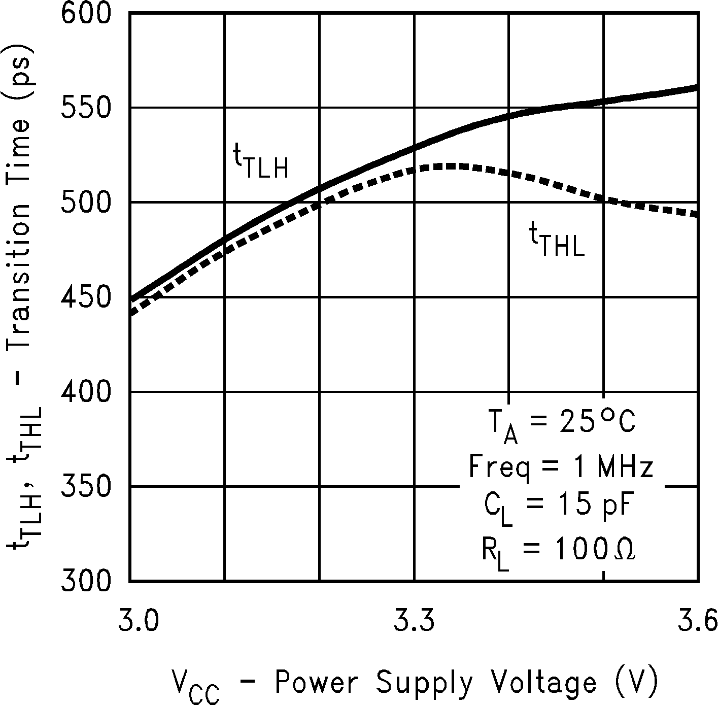 Figure 14. Transition Time vs Power Supply Voltage
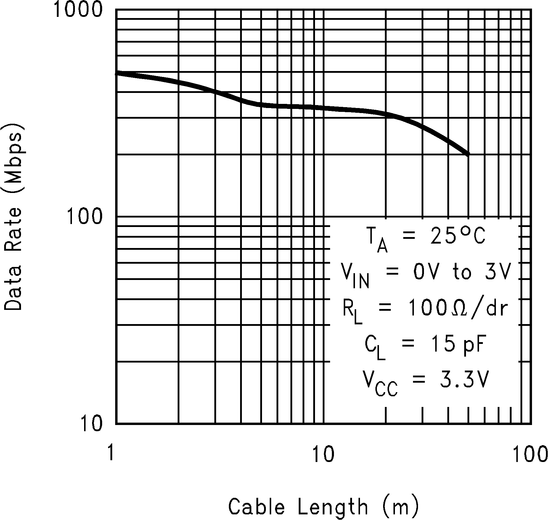 Figure 16. Data Rate vs Cable Length