SNLS414E June 2012 – October 2016 DS90UR910-Q1
PRODUCTION DATA.
- 1 Features
- 2 Applications
- 3 Description
- 4 Revision History
- 5 Pin Configuration and Functions
-
6 Specifications
- 6.1 Absolute Maximum Ratings
- 6.2 ESD Ratings
- 6.3 Recommended Operating Conditions
- 6.4 Thermal Information
- 6.5 Electrical Characteristics: DC
- 6.6 Switching Characteristics: AC
- 6.7 Timing Requirements: Serial Control Bus (CCI and I2C)
- 6.8 Timing Requirements: DC and AC Serial Control Bus (CCI and I2C)
- 6.9 Typical Characteristics
- 7 Detailed Description
- 8 Application and Implementation
- 9 Power Supply Recommendations
- 10Layout
- 11Device and Documentation Support
- 12Mechanical, Packaging, and Orderable Information
6 Specifications
6.1 Absolute Maximum Ratings
over operating free-air temperature range (unless otherwise noted)(1)(2)| MIN | MAX | UNIT | ||
|---|---|---|---|---|
| Supply voltage | VDDA, VDDP, VDDL, VDDCSI (1.8 V) | −0.3 | 2.5 | V |
| VDDIO (1.8-V I/O) | −0.3 | 2.5 | ||
| VDDIO (3.3-V I/O) | –0.3 | 4 | ||
| LVCMOS I/O voltage | −0.3 | VDDIO + 0.3 | V | |
| Receiver input voltage | −0.3 | VDDA + 0.3 | V | |
| CSI-2 output voltage | −0.3 | VDDCSI + 0.3 | V | |
| 40L WQFN package, maximum power dissipation capacity at 25°C (derate above 25°C) | 1/RθJA | mW/°C | ||
| Junction temperature, TJ | 150 | °C | ||
| Storage temperature, Tstg | −65 | 150 | °C | |
(1) Stresses beyond those listed under Absolute Maximum Ratings may cause permanent damage to the device. These are stress ratings only, which do not imply functional operation of the device at these or any other conditions beyond those indicated under Recommended Operating Conditions. Exposure to absolute-maximum-rated conditions for extended periods may affect device reliability.
(2) For soldering specifications, see product folder at www.ti.com and Absolute Maximum Ratings for Soldering (SNOA549).
6.2 ESD Ratings
| VALUE | UNIT | ||||
|---|---|---|---|---|---|
| V(ESD) | Electrostatic discharge | Human body model (HBM), per AEC Q100-002, all pins(1) | ±8000 | V | |
| Charged device model (CDM), per AEC Q100-011, all pins | ±1000 | ||||
| Machine model (MM) | ±250 | ||||
| IEC, powered-up only, RD = 330 Ω, CS = 150 pF |
Air discharge (RIN+, RIN–) | ±30000 | |||
| Contact discharge (RIN+, RIN–) | ±10000 | ||||
| ISO10605, RD = 330 Ω, CS = 150 pF |
Air discharge (RIN+, RIN–) | ±30000 | |||
| Contact discharge (RIN+, RIN–) | ±10000 | ||||
| ISO10605, RD = 2 kΩ, CS = 150 pF or 330 pF |
Air discharge (RIN+, RIN–) | ±30000 | |||
| Contact discharge (RIN+, RIN–) | ±10000 | ||||
(1) AEC Q100-002 indicates HBM stressing is done in accordance with the ANSI/ESDA/JEDEC JS-001 specification.
6.3 Recommended Operating Conditions
over operating free-air temperature range (unless otherwise noted)| MIN | NOM | MAX | UNIT | |||
|---|---|---|---|---|---|---|
| VDDA, VDDP, VDDL, VDDCSI |
Supply voltage | 1.71 | 1.8 | 1.89 | V | |
| VDDIO | LVCMOS supply voltage | 1.8-V I/O | 1.71 | 1.8 | 1.89 | V |
| 3.3-V I/O | 3 | 3.3 | 3.6 | |||
| PCLK | Clock frequency | 10 | 75 | MHz | ||
| VDDn | Supply noise (1.8 V) | 25 | mVP-P | |||
| VDDIO | Supply noise | 1.8-V I/O | 25 | mVP-P | ||
| 3.3-V I/O | 50 | |||||
| TA | Operating free-air temperature | –40 | 25 | 105 | °C | |
6.4 Thermal Information
| THERMAL METRIC(1) | DS90UB921Q-1 | UNIT | |
|---|---|---|---|
| RTA (WQFN) | |||
| 48 PINS | |||
| RθJA | Junction-to-ambient thermal resistance | 30.3 | °C/W |
| RθJC(top) | Junction-to-case (top) thermal resistance | 16.4 | °C/W |
| RθJB | Junction-to-board thermal resistance | 6.3 | °C/W |
| ψJT | Junction-to-top characterization parameter | 0.2 | °C/W |
| ψJB | Junction-to-board characterization parameter | 6.3 | °C/W |
| RθJC(bot) | Junction-to-case (bottom) thermal resistance | 2.2 | °C/W |
(1) For more information about traditional and new thermal metrics, see the Semiconductor and IC Package Thermal Metrics application report.
6.5 Electrical Characteristics: DC
over operating free-air temperature range (unless otherwise noted)(1)(2)(3)| PARAMETER | TEST CONDITIONS | MIN | TYP | MAX | UNIT | ||
|---|---|---|---|---|---|---|---|
| 3.3-V I/O LVCMOS, VDDIO = 3 to 3.6 V (BISTEN, LOCK, PASS, PDB, EQ[3:1], ID[1:0], CONFIG[1:0], GPIO) | |||||||
| VIH | High-level input voltage | VIN = 3 V to 3.6 V | 2.2 | VDDIO | V | ||
| VIL | Low-level input voltage | VIN = 3 V to 3.6 V | GND | 0.8 | V | ||
| IIN | Input current | VIN = 0 V or VDDIO | –15 | 15 | µa | ||
| VOH | High-level output voltage | IOH = −2 mA | 2.4 | VDDIO | V | ||
| VOL | Low-level output voltage | IOL = 2 mA | GND | 0.4 | V | ||
| IOZ | TRI-STATE® output current | PDB = 0 V | –15 | 15 | µa | ||
| 1.8-V I/O LVCMOS, VDDIO = 1.71 to 1.89 V (BISTEN, LOCK, PASS, PDB, EQ[3:1], ID[1:0], CONFIG[1:0], GPIO) | |||||||
| VIH | High-level input voltage | VIN = 1.71 V to 1.89 V | 0.65 × VDDIO | VDDIO | V | ||
| VIL | Low-level input voltage | VIN = 1.71 V to 1.89 V | GND | 0.35 × VDDIO | V | ||
| IIN | Input current | VIN = 0 V or VDDIO | –15 | 15 | µa | ||
| VOH | High-level output voltage | IOH = –2 mA | VDDIO – 0.45 | VDDIO | V | ||
| VOL | Low-level output voltage | IOL = 2 mA | GND | 0.45 | V | ||
| IOZ | TRI-STATE output current | PDB = 0 V | –15 | 15 | µa | ||
| SUPPLY CURRENT | |||||||
| IDD1 | Supply current | Supply current drawn from 1.8-V rail (VDDL, VDDP, VDDA), checker board pattern | VDDL, VDDP, VDDA = 1.89 V, f = 75 MHz (900 Mbps) |
88 | 95 | mA | |
| VDDL, VDDP, VDDA = 1.89 V, f = 10 MHz (120 Mbps) |
38 | ||||||
| IDDTX1 | Supply current | Supply current drawn at VDDCSI, checker board pattern | VDDCSI = 1.89 V, f = 75 MHz (900 Mbps) |
50 | 65 | mA | |
| VDDCSI = 1.89 V, f = 10 MHz (120 Mbps) |
22 | ||||||
| IDDIO1 | Supply current | Supply current drawn at VDDIO, checker board pattern | VDDIO = 1.89 V, f = 75 MHz (900 Mbps) |
10 | mA | ||
| VDDIO = 3.6 V, f = 75 MHz (900 Mbps) |
15 | ||||||
| IDDZ | Supply current at power down mode | Supply current drawn from 1.8-V rail (VDDL, VDDP, VDDA), PDB = 0 V, VDDL, VDDP, VDDA = 1.89 V (all other LVCMOS inputs low) |
5 | mA | |||
| IDDTXZ | Supply current at power down mode | Supply current drawn at VDDCSI, PDB = 0 V, VDDCSI = 1.89 V (all other LVCMOS inputs low) |
5 | mA | |||
| IDDIOZ | Supply current at power down mode | Supply current drawn at VDDIO, PDB = 0 V (all other LVCMOS inputs low) | VDDIO = 1.89 V | 3 | mA | ||
| VDDIO = 3.6 V | 3 | ||||||
| IDDUPLS | Ultra-low power state current | Supply current drawn from 1.8 V at (VDDL, VDDP, VDDA, VDDCSI and VDDIO), VDD = 1.89 V, VDDIO = 3.6 V, PLL off, no change in all input signals, Register: 0x19h = 0x03h 0x01h = 0x02h |
20 | mA | |||
| FPD-LINK II RECEIVER (RIN±) | |||||||
| VTH | Differential input threshold high voltage | VCM = 1.2 V (internal VBIAS) | 50 | mV | |||
| VTL | Differential input threshold low voltage | VCM = 1.2 V (internal VBIAS) | –50 | mV | |||
| VCM | Common mode voltage, internal VBIAS | 1.2 | V | ||||
| IIN | Input current | VIN = 0 V or VDD | −15 | 15 | µa | ||
| RT | Internal termination resistor | Differential across RIN+ and RIN– | 80 | 100 | 120 | Ω | |
| CMLOUT± DRIVER OUTPUT (CMLOUT±) | |||||||
| VOD | Differential output voltage(4) | RL = 100 Ω | 500 | mV | |||
| VOS | Offset voltage, single-ended | RL = 100 Ω | 1.3 | V | |||
| RT | Internal termination resistor | Differential across CMLOUT+ and CMLOUT– | 80 | 100 | 120 | Ω | |
| HSTX DRIVER (DATA0±, DATA1±, CLK±) | |||||||
| VCMTX | HS transmit static common-mode voltage | 150 | 200 | 250 | mV | ||
| |ΔVCMTX(1,0)| | VCMTX mismatch when output is 1 or 0 state | 5 | mV | ||||
| |VOD| | HS transmit differential voltage | 140 | 200 | 270 | mV | ||
| |ΔVOD| | VOD mismatch when output is 1 or 0 state | 10 | mV | ||||
| VOHHS | HS output high voltage | 360 | mV | ||||
| ZOS | Single ended output impedance | 40 | 50 | 62.5 | Ω | ||
| ΔZOS | Mismatch in single ended output impedance | 10% | |||||
| LPTX DRIVER (DATA0±, DATA1±, CLK±) | |||||||
| VOH | Output high level(5) | 1.1 | 1.2 | 1.3 | V | ||
| VOL | Output low level | −50 | 50 | mV | |||
| ZOLP | Output impedance | 110 | Ω | ||||
(1) Current into device pins is defined as positive. Current out of a device pin is defined as negative. Voltages are referenced to ground except VOD, ΔVOD, VTH and VTL which are differential voltages.
(2) Typical values represent most likely parametric norms at VDD = 3.3 V, TA = 25°C, and at the recommended operation conditions at the time of product characterization and are not ensured.
(3) The Electrical Characteristics tables list ensured specifications in Recommended Operating Conditions except as otherwise modified or specified by the Electrical Characteristics Conditions and/or Notes. Typical specifications are estimations only and are not ensured.
(4) Voltage difference compared to the DC average common mode potential.
(5) Specification is ensured by characterization.
6.6 Switching Characteristics: AC
over operating free-air temperature range (unless otherwise noted)| PARAMETER | TEST CONDITIONS | MIN | TYP | MAX | UNIT | ||
|---|---|---|---|---|---|---|---|
| FPD-LINK II RECEIVER (RIN±) | |||||||
| tIJT | Input jitter tolerance, see Figure 1 |
EQ = OFF, PCLK = 65 MHz |
jitter freq < 2 MHz | 0.9 | UI(1) | ||
| jitter freq > 6 MHz | 0.5 | UI | |||||
| tDDLT | Deserializer lock time see Figure 2 |
PCLK = 75 MHz | 10 | ms | |||
| HSTX DRIVER (DATA0±, DATA1±, CLK±) | |||||||
| HSTXDBR | Data bit rate | DATA0±, DATA1±, PCLK = 10 to 75 MHz(2) | 120 | PCLK × 12 | 900 | Mbps | |
| fCLK | DDR Clock frequency | CLK±, PCLK = 10 to 75 MHz(2) | 60 | PCLK × 6 | 450 | MHz | |
| ΔVCMTX(HF) | Common mode voltage variations HF | Common-level variations above 450 MHz(2) | 15 | mVRMS | |||
| ΔVCMTX(LF) | Common mode voltage variations LF | Common-level variations between 50 to 450 MHz(2) | 25 | mVPEAK | |||
| tRHS | Rise time HS | 20% to 80% rise time(3) | 0.3 | UIINST | |||
| 150 | ps | ||||||
| tFHS | Fall time HS | 20% to 80% rise time(3) | 0.3 | UIINST | |||
| 150 | ps | ||||||
| SDDTX | TX differential return loss(2) | fLPMAX | –18 | dB | |||
| fH | –12 | dB | |||||
| fMAX | –6 | dB | |||||
| SCCTX | TX common mode return loss(2) | fLPMAX to fMAX | –6 | dB | |||
| LPTX DRIVER (DATA0±, DATA1±, CLK±)(4) | |||||||
| tRLP | Rise time | LP 15% to 85% rise time CLOAD = 70 pF lumped capacitance |
25 | ns | |||
| tFLP | Fall time | LP 15% to 85% fall time CLOAD = 70 pF lumped capacitance |
25 | ns | |||
| tREOT | Post-EoT rise and fall time | 30% to 85% rise time and fall time(2) | 35 | ns | |||
| tLP-PULSE-TX | Pulse width of the LP exclusive-OR clock | First LP exclusive-OR clock pulse after Stop state or last pulse before Stop state (2) | 40 | ns | |||
| All other pulses(2) | 20 | ns | |||||
| tLP-PER-TX | Period of the LP exclusive-OR clock(2) | 90 | ns | ||||
| σV/σtSR | Slew rate | CLOAD = 0 pF(5)(4)(5) | 500 | mV/ns | |||
| CLOAD = 5 pF(5)(4)(5) | 300 | mV/ns | |||||
| CLOAD = 20 pF(5)(4)(5) | 250 | mV/ns | |||||
| CLOAD = 70 pF(3)(4)(5) | 150 | mV/ns | |||||
| CLOAD = 0 to 70 pF (falling edge only)(3)(4)(5)(6) | 30 | mV/ns | |||||
| CLOAD = 0 to 70 pF (rising edge only)(3)(4)(5) | 30 | mV/ns | |||||
| CLOAD = 0 to 70 pF (rising edge only)(3)(4)(7)(8) | 30 – 0.075 × (VO,INST – 700) | mV/ns | |||||
| CLOAD | Load capacitance(4) | 0 | 70 | pF | |||
| DATA-CLOCK TIMING SPECIFICATIONS (DATA0±, DATA1±, CLK±) | |||||||
| UIINST | Instantaneous unit interval, see Figure 3 |
PCLK = 10 to 75 MHz(9) | 1/(PCLK × 12) | ns | |||
| tSKEW(TX) | Data to clock skew see Figure 3 |
Skew between clock and data from ideal center(2) | 0.5 – 0.15 | 0.5 | 0.5 + 0.15 | UIINST | |
| CSI-2 TIMING SPECIFICATIONS (DATA0±, DATA1±, CLK±)(2) ( see Figure 4 and Figure 5) | |||||||
| tCLK–POST | HS exit | 60 + 52 × UIINST | ns | ||||
| tCLK–PRE | Time HS clock shall be driver prior to any associated Data Lane beginning the transition from LP to HS mode | 8 | UIINST | ||||
| tCLK–PREPARE | Clock lane HS entry | 38 | 95 | ns | |||
| tCLK–SETTLE | Time interval during which the HS receiver shall ignore any clock lane HS transitions | 95 | 300 | ns | |||
| tCLK–TERM-EN | Time-out at clock lane display module to enable HS termination | 38 | ns | ||||
| tCLK–TRAIL | Time that the transmitter drives the HS-0 state after the last payload clock bit of a HS transmission burst | 30 | ns | ||||
| tCLK–PREPARE + tCLK–ZERO | TCLK–PREPARE + time that the transmitter drives the HS-0 state prior to starting the clock | 300 | ns | ||||
| tD-TERM-EN (10) | Time for the data lane receiver to enable the HS line termination | 35 + 4 × UIINST | ns | ||||
| tLPX | Transmitted length of LP state | 50 | ns | ||||
| tHS-PREPARE | Data lane HS entry | 40 + 4 × UIINST | 85 + 6 × UIINST | ns | |||
| tHS-PREPARE + tHS-ZERO | tHS-PREPARE + time that the transmitter drives the HS-0 state prior to transmitting the sync sequence | 145 + 10 × UIINST | ns | ||||
| tHS-SETTLE | Interval HS receiver shall ignore any data lane HS transitions | 85 + 6 × UIINST | 145 + 10 × UIINST | ns | |||
| tHS-TRAIL | Data lane HS exit | 60 + 4 × UIINST | ns | ||||
| tEOT | Transmitted time interval from the start of tHS-TRAIL to the start of the LP-11 state following a HS burst | 105 + 12 × UIINST | ns | ||||
| tHS-EXIT | Time that the transmitter drives LP-11 following a HS burst. | 100 | ns | ||||
| tWAKEUP | Recovery time from ultra-low power state (ULPS) | 1 | ms | ||||
(1) UI is equivalent to one serialized data bit width (1UI = 1 / 28 × PCLK). The UI scales with PCLK frequency.
(2) Specification is ensured by design and is not tested in production.
(3) Specification is ensured by characterization.
(4) CLOAD includes the low-frequency equivalent transmission line capacitance. The capacitance of TX and RX are assumed to always be <10 pF. The distributed line capacitance can be up to 50 pF for a transmission line with 2-ns delay.
(5) Measured as average across any 50 mV segment of the output signal transition.
(6) When the output voltage is between 400 mV and 930 mV.
(7) Where VO,INST is the instantaneous output voltage, VDP or VDN, in millivolts.
(8) When the output voltage is between 700 mV and 930 mV.
(9) UIINST is equal to 1 / (12 × PCLK), where PCLK is the fundamental frequency for data transmission.
(10) This parameter value can be lower then TLPX due to differences in rise versus fall signal slopes and trip levels and mismatches between Dp and Dn LP transmitters. Any LP exclusive-OR pulse observed during HS EoT (transition from HS level to LP-11) is glitch behavior as described in D-PHY ver 1.00.00.
6.7 Timing Requirements: Serial Control Bus (CCI and I2C)
over operating free-air temperature range (unless otherwise noted; see Figure 7)(1)| MIN | NOM | MAX | UNIT | |||
|---|---|---|---|---|---|---|
| fSCL | SCL clock frequency | Standard mode | >0 | 100 | kHz | |
| Fast mode | >0 | 400 | kHz | |||
| tLOW | SCL low period | Standard mode | 4.7 | µs | ||
| Fast mode | 1.3 | µs | ||||
| tHIGH | SCL high period | Standard mode | 4 | µs | ||
| Fast mode | 0.6 | µs | ||||
| tHD;STA | Hold time for a start or a repeated start condition | Standard mode | 4 | µs | ||
| Fast mode | 0.6 | µs | ||||
| tSU;STA | Set-up time for a start or a repeated start condition | Standard mode | 4.7 | µs | ||
| Fast mode | 0.6 | µs | ||||
| tHD;DAT | Data hold time | Standard mode | 0 | 3.45 | µs | |
| Fast mode | 0 | 0.9 | µs | |||
| tSU;DAT | Data set-up time | Standard mode | 250 | ns | ||
| Fast mode | 100 | ns | ||||
| tSU;STO | Set-up time for STOP condition | Standard mode | 4 | µs | ||
| Fast mode | 0.6 | µs | ||||
| tBµF | Bus Free Time between STOP and START |
Standard mode | 4.7 | µs | ||
| Fast mode | 1.3 | µs | ||||
| tr | SCL and SDA rise time | Standard mode | 1000 | ns | ||
| Fast mode | 300 | ns | ||||
| tf | SCL and SDA fall time | Standard mode | 300 | ns | ||
| Fast mode | 300 | ns | ||||
(1) Recommended Input Timing Requirements are input specifications and not tested in production.
6.8 Timing Requirements: DC and AC Serial Control Bus (CCI and I2C)
over operating free-air temperature range (unless otherwise noted; see Figure 7)| MIN | NOM | MAX | UNIT | |||
|---|---|---|---|---|---|---|
| VIH | Input high level voltage | SDA and SCL | 0.65 × VDDIO | VDDIO | V | |
| VIL | Input low level voltage | SDA and SCL | GND | 0.35 × VDDIO | V | |
| VHY | Input hysteresis | Fast mode, 3.3-V I/O(1) | 0.05 × VDDIO | mV | ||
| Fast mode, 1.8 V I/O | 0.1 × VDDIO | mV | ||||
| VOL | Output low level voltage | SDA, IOL = 1.5 mA | 0 | 0.4 | V | |
| tR | SDA rise time – READ | Total capacitance of one bus line, Cb ≤ 400 pF |
300 | ns | ||
| tF | SDA fall time – READ | Standard mode | 1000 | ns | ||
| Fast mode | 300 | ns | ||||
| tSU;DAT | Set-up time – READ | Standard mode | 250 | ns | ||
| Fast mode | 100 | ns | ||||
| tHD;DAT | Hold-up time – READ | 0 | ns | |||
| tSP | Input filter | Fast mode | 50 | ns | ||
| Cin | Input capacitance | SDA and SCL | 5 | pF | ||
(1) Specification is ensured by characterization.
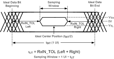 Figure 1. Receiver Input Jitter Tolerance
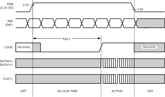 Figure 2. Deserializer PLL Lock Time
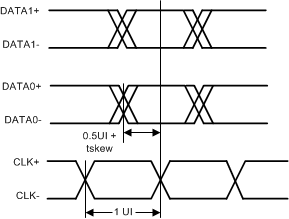 Figure 3. Clock and Data Timing in HS Transmission
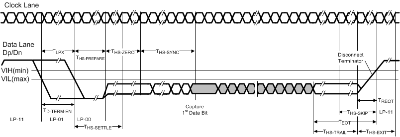 Figure 4. High-Speed Data Transmission Burst
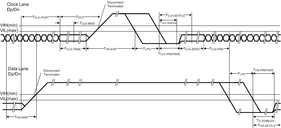 Figure 5. Switching the Clock Lane Between Clock Transmission and Low-Power Mode
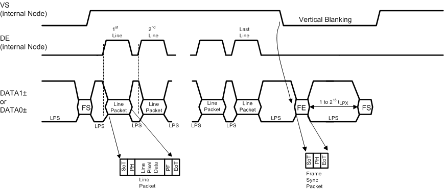 Figure 6. Long Line Packets and Short Frame Sync Packets
 Figure 7. Serial Control Bus Timing Diagram
6.9 Typical Characteristics
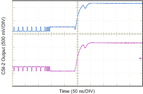 Figure 8. CSI-2 D0± End of Transmission
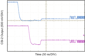 Figure 9. CSI-2 D0± Start of Transmission