DS90UB927Q-Q1 5-MHz to 85-MHz 24-bit Color FPD-Link III Serializer With Bidirectional Control Channel
1 Features
- Bidirectional Control Channel Interface with I2C-compatible Serial Control Bus
- Low EMI FPD-Link Video Input
- Supports High Definition (720p) Digital Video Format
- 5-MHz to 85-MHz PCLK Supported
- RGB888 + VS, HS, DE and I2S Audio Supported
- Up to 4 I2S Digital Audio Inputs for Surround Sound Applications
- 4 Bidirectional GPIO Channels with 2 Dedicated Pins
- Single 3.3-V Supply with 1.8-V or 3.3-V Compatible LVCMOS I/O Interface
- AC-Coupled STP Interconnect Up to 10 Meters
- DC-Balanced and Scrambled Data With Embedded Clock
- Supports Repeater Application
- Internal Pattern Generation
- Low Power Modes Minimize Power Dissipation
- Automotive Grade Product: AEC-Q100 Grade 2 Qualified
- >8-kV HBM and ISO 10605 ESD Rating
- Backward Compatible Modes
2 Applications
- Automotive Displays for Navigation
- Rear Seat Entertainment Systems
- Automotive Driver Assistance
- Automotive Megapixel Camera Systems
3 Description
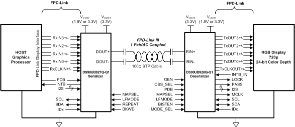
The DS90UB927Q-Q1 serializer, in conjunction with a DS90UB928Q-Q1 or DS90UB926Q-Q1 deserializer, provides a complete digital interface for concurrent transmission of high-speed video, audio, and control data for automotive display and image sensing applications.
The chipset is ideally suited for automotive video display systens with HD formats and automotive vision systems with megapixel resolutions. The DS90UB927Q-Q1 incorporates an embedded bidirectional control channel and low latency GPIO controls. This device translates a FPD-Link video interface into a single-pair high-speed serialized interface. The FPD-Link III serial bus scheme supports full duplex, high speed forward channel data transmission and low-speed back channel communication over a single differential link. Consolidation of audio, video, and control data over a single differential pair reduces the interconnect size and weight, while also eliminating skew issues and simplifying system design.
The DS90UB927Q-Q1 serializer embeds the clock and level shifts the signals to high-speed differential signaling. Up to 24 RGB data bits are serialized along with three video control signals, and up to four I2S data inputs.
The FPD-Link data interface allows for easy interfacing with data sources while also minimizing EMI and bus width. EMI on the high-speed FPD-Link III bus is minimized using low voltage differential signaling, data scrambling and randomization, and DC-balancing.
Device Information(1)
| PART NUMBER | PACKAGE | BODY SIZE (NOM) |
|---|---|---|
| DS90UB927Q-Q1 | WQFN (40) | 6.00 mm x 6.00 mm |
- For all available packages, see the orderable addendum at the end of the datasheet.
Application Diagram
4 Revision History
Changes from C Revision (October 2012) to D Revision
- Added ESD Ratings table, Feature Description section, Device Functional Modes, Application and Implementation section, Power Supply Recommendations section, Layout section, Device and Documentation Support section, and Mechanical, Packaging, and Orderable Information sectionGo
Changes from B Revision (June 2012) to C Revision
- Changed layout of National data sheet to tI formatGo
5 Pin Configuration and Functions
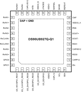
Pin Functions
| PIN | I/O | DESCRIPTION | |
|---|---|---|---|
| NAME | NO. | ||
| FPD-LINK INPUT INTERFACE | |||
| RxCLKIN- | 35 | I, LVDS | Inverting LVDS Clock Input The pair requires external 100-Ω differential termination for standard LVDS levels |
| RxCLKIN+ | 36 | I, LVDS | True LVDS Clock Input The pair requires external 100-Ω differential termination for standard LVDS levels |
| RxIN[3:0]- | 37, 33, 31, 29 |
I, LVDS | Inverting LVDS Data Inputs Each pair requires external 100-Ω differential termination for standard LVDS levels |
| RxIN[3:0]+ | 38, 34, 32, 30 |
I, LVDS | True LVDS Data Inputs Each pair requires external 100-Ω differential termination for standard LVDS levels |
| LVCMOS PARALLEL INTERFACE | |||
| BKWD | 22 | I, LVCMOS with pulldown |
Backward Compatible Mode Select BKWD = 0, interfacing to DS90UH926/8Q-Q1 (Default) BKWD = 1, interfacing to DS90UR906/8Q-Q1, DS90UR916Q Requires a 10-kΩ pullup if set HIGH |
| GPIO[1:0] | 40, 39 | I/O, LVCMOS with pulldown |
General Purpose I/O See Table 1 |
| I2S_DA I2S_DB I2S_DC I2S_DD |
3 4 5 6 |
I, LVCMOS with pulldown |
Digital Audio Interface I2S Data Inputs Shared with GPIO_REG6, GPIO_REG5, GPIO2, GPIO3 |
| I2S_WC I2S_CLK |
1 2 |
I, LVCMOS with pulldown |
Digital Audio Interface I2S Word Clock and I2S Bit Clock Inputs Shared with GPIO_REG7 and GPIO_REG8 (Table 3) |
| LFMODE | 25 | I, LVCMOS with pulldown |
Low Frequency Mode Select LFMODE = 0, 15 MHz ≤ RxCLKIN ≤ 85 MHz (Default) LFMODE = 1, 5 MHz ≤ RxCLKIN < 15 MHz Requires a 10-kΩ pullup if set HIGH |
| MAPSEL | 23 | I, LVCMOS with pulldown |
FPD-Link Input Map Select MAPSEL = 0, LSBs on RxIN3± (Default) MAPSEL = 1, MSBs on RxIN3± See Figure 19 and Figure 20 Requires a 10-kΩ pullup if set HIGH |
| REPEAT | 21 | I, LVCMOS with pulldown |
Repeater Mode Select REPEAT = 0, Repeater Mode disabled (Default) REPEAT = 1, Repeater Mode enabled Requires a 10-kΩ pullup if set HIGH |
| OPTIONAL PARALLEL INTERFACE | |||
| GPIO[3:2] | 6, 5 | I/O, LVCMOS with pulldown |
General Purpose I/O Shared with I2S_DD and I2S_DC (See Table 1) |
| GPIO_REG [8:5] |
2, 1, 3, 4 | I/O, LVCMOS with pulldown |
Register-Only General Purpose I/O Shared with I2S_CLK, I2S_WC, I2S_DA, I2S_DB (See Table 2) |
| CONTROL AND CONFIGURATION | |||
| IDx | 11 | I, Analog | I2C Address Select External pullup to VDD33 is required under all conditions. DO NOT FLOAT. Connect to external pullup to VDD33 and pulldown to GND to create a voltage divider. See Figure 25 and Table 4 |
| PDB | 18 | I, LVCMOS with pulldown |
Power-down Mode Input Pin Must be driven or pulled up to VDD33. Refer to Power Supply Recommendations. PDB = H, device is enabled (normal operation) PDB = L, device is powered down. When the device is in the powered down state, the Driver Outputs are both HIGH, the PLL is shutdown, and IDD is minimized. Control Registers are RESET. |
| SCL | 9 | I/O, LVCMOS Open Drain |
I2C Clock Input / Output Interface Must have an external pullup to VDD33. DO NOT FLOAT. Recommended pullup: 4.7 kΩ. |
| SDA | 10 | I/O, LVCMOS Open Drain |
I2C Data Input / Output Interface Must have an external pullup to VDD33. DO NOT FLOAT. Recommended pullup: 4.7 kΩ. |
| STATUS | |||
| INTB | 27 | O, LVCMOS Open Drain |
Interrupt INTB = H, normal INTB = L, Interrupt request Recommended pullup: 4.7 kΩ to VDDIO. DO NOT FLOAT. |
| FPD-LINK III SERIAL INTERFACE | |||
| CMF | 20 | Analog | Common Mode Filter. Connect 0.1 µF to GND (required) |
| DOUT- | 16 | I/O, LVDS | Inverting Output The output must be AC-coupled with a 0.1-µF capacitor. |
| DOUT+ | 17 | I/O, LVDS | True Output The output must be AC-coupled with a 0.1-µF capacitor. |
| POWER(1) AND GROUND | |||
| GND | DAP | Ground | Large metal contact at the bottom center of the device package Connect to the ground plane (GND) with at least 9 vias. |
| VDD33_A VDD33_B |
19 26 |
Power | Power to on-chip regulator 3.0 V - 3.6 V. Each pin requires a 4.7-µF capacitor to GND |
| VDDIO | 7, 24 | Power | LVCMOS I/O Power 1.8 V ±5% OR 3.0 V - 3.6 V. Each pin requires 4.7-µF capacitor to GND |
| REGULATOR CAPACITOR | |||
| CAPL12 | 8 | CAP | Decoupling capacitor connection for on-chip regulator Requires two 4.7-µF decoupling capacitors to GND |
| CAPP12 CAPHS12 CAPLVD12 |
12 14 28 |
CAP | Decoupling capacitor connection for on-chip regulator Each requires a 4.7-µF decoupling capacitor to GND. |
| OTHER | |||
| RES[1:0] | 15, 13 | GND | Reserved Connect to GND. |
6 Specifications
6.1 Absolute Maximum Ratings(2)(1)(3)
| MIN | MAX | UNIT | ||
|---|---|---|---|---|
| Supply Voltage – VDD33 | −0.3 | 4.0 | V | |
| Supply Voltage – VDDIO | −0.3 | 4.0 | V | |
| LVCMOS I/O Voltage | −0.3 | VDDIO + 0.3 | V | |
| Serializer Output Voltage | −0.3 | 2.75 | V | |
| Junction Temperature | 150 | °C | ||
| Storage Temperature, Tstg | −65 | 150 | °C | |
6.2 ESD Ratings
| VALUE | UNIT | |||||
|---|---|---|---|---|---|---|
| V(ESD) | Electrostatic discharge | Human body model (HBM), per AEC Q100-002(1) | ±8000 | V | ||
| Charged device model (CDM), per AEC Q100-011 | ±1250 | |||||
| Machine model (MM) | ±250 | |||||
| (IEC 61000-4-2, powered-up only) RD = 330 Ω, CS = 150 pF |
Air Discharge (Pin 16 and 17) |
±15000 | ||||
| Contact Discharge (Pin 16 and 17) |
±8000 | |||||
| (ISO 10605) RD = 330 Ω, CS = 150 pF/330 pF RD = 2 kΩ, CS = 150 pF/330 pF |
Air Discharge (Pin 16 and 17) |
±15000 | ||||
| Contact Discharge (Pin 16 and 17) |
±8000 | |||||
6.3 Recommended Operating Conditions
over operating free-air temperature range (unless otherwise noted)| MIN | NOM | MAX | UNIT | ||
|---|---|---|---|---|---|
| Supply Voltage (VDD33) | 3.0 | 3.3 | 3.6 | V | |
| LVCMOS Supply Voltage (VDDIO)(2) | Connect VDDIO to 3.3 V and use 3.3-V IOs | 3.0 | 3.3 | 3.6 | V |
| Connect VDDIO to 1.8 V and use 1.8-V IOs | 1.71 | 1.8 | 1.89 | ||
| Operating Free Air Temperature (TA) | −40 | +25 | +105 | °C | |
| PCLK Frequency | 5 | 85 | MHz | ||
| Supply Noise(1) | 100 | mVP-P | |||
6.4 Thermal Information
| THERMAL METRIC(1) | DS90UB927Q-Q1 | UNIT | |
|---|---|---|---|
| RTA (WQFN) | |||
| 40 PINS | |||
| RθJA | Junction-to-ambient thermal resistance | 29.0 | °C/W |
| RθJC(top) | Junction-to-case (top) thermal resistance | 14.4 | |
| RθJB | Junction-to-board thermal resistance | 5.1 | |
| ψJT | Junction-to-top characterization parameter | 0.2 | |
| ψJB | Junction-to-board characterization parameter | 5.1 | |
| RθJC(bot) | Junction-to-case (bottom) thermal resistance | 1.4 | |
6.5 DC Electrical Characteristics
Over recommended operating supply and temperature ranges unless otherwise specified.(1)(2)(3)| PARAMETER | TEST CONDITIONS | PIN / FREQ | MIN | NOM | MAX | UNIT | ||
|---|---|---|---|---|---|---|---|---|
| LVCMOS I/O | ||||||||
| VIH | High Level Input Voltage | VDDIO = 3.0 V to 3.6 V(4) | PDB | 2.0 | VDDIO | V | ||
| VIL | Low Level Input Voltage | VDDIO = 3.0 V to 3.6 V(4) | GND | 0.8 | V | |||
| IIN | Input Current | VIN = 0 V or VDDIO = 3.0 V to 3.6 V(4) | −15 | ±1 | +15 | μA | ||
| VIH | High Level Input Voltage | VDDIO = 3.0 V to 3.6 V | GPIO[1:0] I2S_CLK I2S_WC I2S_D[A,B,C,D] LFMODE MAPSEL BKWD REPEAT |
2.0 | VDDIO | V | ||
| VDDIO = 1.71 V to 1.89 V | 0.65*VDDIO | VDDIO | V | |||||
| VIL | Low Level Input Voltage | VDDIO = 3.0 V to 3.6 V | GND | 0.8 | V | |||
| VDDIO = 1.71 V to 1.89 V | GND | 0.35* VDDIO |
V | |||||
| IIN | Input Current | VIN = 0 V or VDDIO | VDDIO = 3.0 V to 3.6 V | −15 | ±1 | +15 | μA | |
| VDDIO = 1.71 V to 1.89 V | −15 | ±1 | +15 | μA | ||||
| VOH | High Level Output Voltage | IOH = −4 mA | VDDIO = 3.0 V to 3.6 V | GPIO[3:0], GPO_REG[8:5] | 2.4 | VDDIO | V | |
| VDDIO = 1.71 V to 1.89 V | VDDIO - 0.45 | VDDIO | V | |||||
| VOL | Low Level Output Voltage | IOL = +4 mA | VDDIO = 3.0 V to 3.6 V | GND | 0.4 | V | ||
| VDDIO = 1.71 V to 1.89 V | GND | 0.45 | V | |||||
| IOS | Output Short Circuit Current | VOUT = 0 V | −55 | mA | ||||
| IOZ | Tri-state Output Current | VOUT = 0 V or VDDIO, PDB = L | −15 | +15 | μA | |||
| FPD-LINK LVDS RECEIVER | ||||||||
| VTH | Threshold High Voltage | VCM = 1.2 V | RxCLKIN± RxIN[3:0]± |
+100 | mV | |||
| VTL | Threshold Low Voltage | −100 | mV | |||||
| |VID| | Differential Input Voltage Swing | 200 | 600 | mV | ||||
| VCM | Common Mode Voltage | 0 | 1.2 | 2.4 | V | |||
| IIN | Input Current | −10 | +10 | μA | ||||
| FPD-LINK III CML DRIVER | ||||||||
| VODp-p | Differential Output Voltage (DOUT+) – (DOUT-) |
RL = 100 Ω (Figure 1) | DOUT± | 800 | 1000 | 1200 | mVp-p | |
| ΔVOD | Output Voltage Unbalance | 1 | 50 | mV | ||||
| VOS | Offset Voltage – Single-ended | RL = 100 Ω (Figure 1) | 2.5-0.25* VODp-p (TYP) |
V | ||||
| ΔVOS | Offset Voltage Unbalance Single-ended |
1 | 50 | mV | ||||
| IOS | Output Short Circuit Current | DOUT+/- = 0 V, PDB = L or H(5) | −30 | mA | ||||
| RT | Internal Termination Resistance - Differential | 80 | 100 | 120 | Ω | |||
| SUPPLY CURRENT | ||||||||
| IDD1 | Supply Current RL = 100 Ω, PCLK = 85 MHz |
Checkerboard Pattern (Figure 8) | VDD33= 3.6 V | 135 | 160 | mA | ||
| IDDIO1 | VDDIO = 3.6 V | 100 | 500 | μA | ||||
| VDDIO = 1.89 V | 200 | 600 | μA | |||||
| IDD2 | Random Pattern PRBS7 |
VDD33= 3.6 V | 133 | mA | ||||
| IDDIO2 | VDDIO = 3.6 V | 100 | μA | |||||
| VDDIO = 1.89 V | 100 | μA | ||||||
| IDDS | Supply Current – Remote Auto Power Down | reg_0x01[7]=1, Back channel Idle | VDD33 = 3.6 V | 1.2 | 2.4 | mA | ||
| IDDIOS | VDDIO = 3.6 V | 4 | 30 | μA | ||||
| VDDIO = 1.89 V | 5 | 30 | μA | |||||
| IDDZ | Supply Current – Power Down | PDB = 0 V, All other LVCMOS inputs = 0 V | VDD33 = 3.6 V | 1 | 2.2 | mA | ||
| IDDIOZ | VDDIO = 3.6 V | 8 | 20 | μA | ||||
| VDDIO = 1.89 V | 4 | 20 | μA | |||||
6.6 AC Electrical Characteristics
over operating free-air temperature range (unless otherwise noted)(1)(2)(3)| PARAMETER | TEST CONDITIONS | PIN / FREQ | MIN | TYP | MAX | UNIT | |
|---|---|---|---|---|---|---|---|
| FPD-LINK LVDS INPUT | |||||||
| tRSP | Receiver Strobe Position | See Figure 4 | RxCLKIN±, RXIN[3:0]± | 0.25 | 0.5 | 0.75 | UI |
| AC ELECTRICAL CHARACTERISTICS - FPD-LINK III CML IO | |||||||
| tLHT | CML Output Low-to-High Transition Time | See Figure 3 | DOUT+, DOUT- | 100 | 140 | ps | |
| tHLT | CML Output High-to-Low Transition Time | 100 | 140 | ps | |||
| tPLD | Serializer PLL Lock Time |
See Figure 5(10) | PCLK = 5MHz to 85MHz |
5 | ms | ||
| tSD | Delay — Latency | See Figure 6 | 146*T | ns | |||
| tTJIT | Output Total Jitter, Bit Error Rate ≤1E-9 Figure 7(5)(4)(8)(9)(6) |
Checkerboard Pattern PCLK=5 MHz, Figure 8 |
RxCLKIN± | 0.17 | 0.2 | UI | |
| Checkerboard Pattern PCLK=85 MHz, Figure 8 |
0.26 | 0.29 | UI | ||||
| tIJIT | Input Jitter Tolerance, Bit Error Rate ≤1E-9(4)(7) | f/40 < Jitter Freq < f/20, DES = DS90UB926Q-Q1 |
RxCLKIN±, f = 78 MHz |
0.6 | UI | ||
| f/40 < Jitter Freq < f/20, DES = DS90UB928Q-Q1 |
0.5 | UI | |||||
| AC ELECTRICAL CHARACTERISTICS - I2S RECEIVER | |||||||
| TI2S | I2S Clock Period (5)(11) |
RxCLKIN± f=5 MHz to 85 MHz | I2S_CLK, PCLK = 5 MHz to 85 MHz |
>4/PCLK or >77 |
ns | ||
| THC | I2S Clock High Time (11) |
I2S_CLK | 0.35 | TI2S | |||
| TLC | I2S Clock Low Time (11) |
I2S_CLK | 0.35 | TI2S | |||
| tsr | I2S Set-up Time |
I2S_WC I2S_D[A,B,C,D] |
0.2 | TI2S | |||
| thtr | I2S Hold Time |
I2S_WC I2S_D[A,B,C,D] |
0.2 | TI2S | |||
| AC ELECTRICAL CHARACTERISTICS - OTHER I/O | |||||||
| tGPIO,FC | GPIO Pulse Width, Forward Channel | GPIO[3:0], PCLK = 5 MHz to 85 MHz |
>2/PCLK | s | |||
| tGPIO,BC | GPIO Pulse Width, Back Channel | GPIO[3:0] | 20 | µs | |||
| DC AND AC SERIAL CONTROL BUS CHARACTERISTICS | |||||||
| tR | SDA RiseTime – READ | SDA, RPU = 10 kΩ, Cb ≤ 400 pF, Figure 9 | 430 | ns | |||
| tF | SDA Fall Time – READ | 20 | ns | ||||
6.7 Electrical Characteristics: DC and AC Serial Control Bus
Over 3.3-V supply and temperature ranges unless otherwise specified.(1)(2)(3)| PARAMETER | TEST CONDITIONS | MIN | TYP | MAX | UNIT | |
|---|---|---|---|---|---|---|
| VIH | Input High Level | SDA and SCL | 0.7*VDDIO | VDD33 | V | |
| VIL | Input Low Level Voltage | SDA and SCL | GND | 0.3*VDD33 | V | |
| VHY | Input Hysteresis | >50 | mV | |||
| VOL | SDA or SCL, IOL = 1.25 mA | 0 | 0.36 | V | ||
| Iin | SDA or SCL, Vin = VDDIO or GND | -10 | +10 | µA | ||
| Cin | Input Capacitance | SDA or SCL | <5 | pF | ||
6.8 Timing Requirements for the Serial Control Bus
Over 3.3-V supply and temperature ranges unless otherwise specified.(1)(2)(3)| MIN | NOM | MAX | UNIT | |||
|---|---|---|---|---|---|---|
| fSCL | SCL Clock Frequency | Standard Mode | 0 | 100 | kHz | |
| Fast Mode | 0 | 400 | ||||
| tLOW | SCL Low Period | Standard Mode | 4.7 | µs | ||
| Fast Mode | 1.3 | |||||
| tHIGH | SCL High Period | Standard Mode | 4.0 | µs | ||
| Fast Mode | 0.6 | |||||
| tHD;STA | Hold time for a start or a repeated start condition (Figure 9) | Standard Mode | 4.0 | µs | ||
| Fast Mode | 0.6 | |||||
| tSU:STA | Set Up time for a start or a repeated start condition (Figure 9) | Standard Mode | 4.7 | µs | ||
| Fast Mode | 0.6 | |||||
| tHD;DAT | Data Hold Time (Figure 9) |
Standard Mode | 0 | 3.45 | µs | |
| Fast Mode | 0 | 0.9 | ||||
| tSU;DAT | Data Set Up Time (Figure 9) |
Standard Mode | 250 | ns | ||
| Fast Mode | 100 | |||||
| tSU;STO | Set Up Time for STOP Condition (Figure 9) |
Standard Mode | 4.0 | µs | ||
| Fast Mode | 0.6 | |||||
| tBUF | Bus Free Time Between STOP and START (Figure 9) |
Standard Mode | 4.7 | µs | ||
| Fast Mode | 1.3 | |||||
| tr | SCL & SDA Rise Time, (Figure 9) | Standard Mode | 1000 | ns | ||
| Fast Mode | 300 | |||||
| tf | SCL & SDA Fall Time, (Figure 9) |
Standard Mode | 300 | ns | ||
| Fast mode | 300 | |||||
6.9 Timing Requirements - DC and AC Serial Control Bus Characteristics
| MIN | TYP | MAX | UNIT | ||
|---|---|---|---|---|---|
| tSU;DAT | Set Up Time – READ (Figure 9) | 560 | ns | ||
| tHD;DAT | Hold Up Time – READ (Figure 9) | 615 | ns | ||
| tSP | Input Filter | 50 | ns | ||
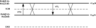 Figure 1. FPD-Link DC VTH/VTL Definition
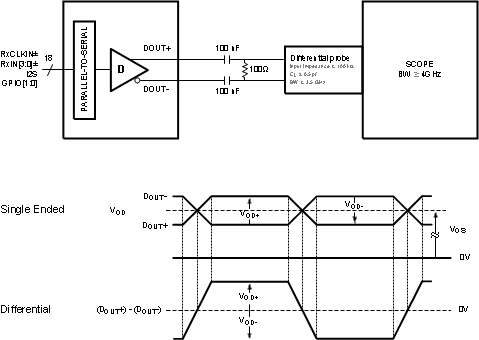 Figure 2. Serializer VOD DC Output
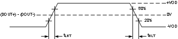 Figure 3. Output Transition Times
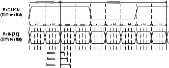 Figure 4. FPD-Link Input Strobe Position
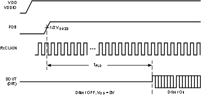 Figure 5. Serializer Lock Time
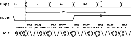 Figure 6. Latency Delay
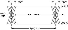 Figure 7. CML Serializer Output Jitter
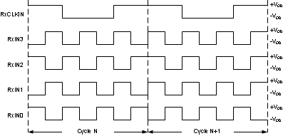 Figure 8. Checkerboard Data Pattern
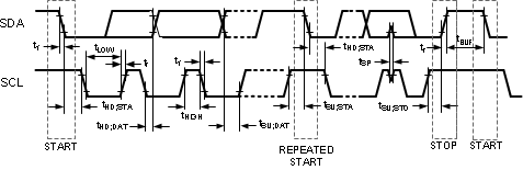 Figure 9. Serial Control Bus Timing Diagram
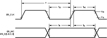 Figure 10. I2S Timing Diagram
6.10 Typical Characteristics
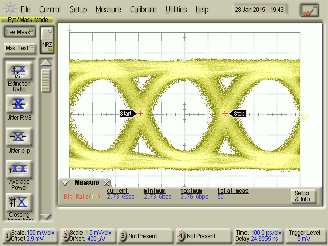 Figure 11. Serializer Eye with 78 MHz Input Clock
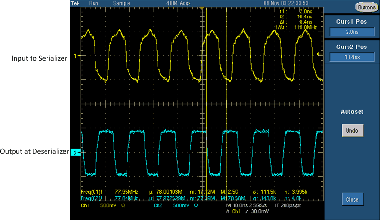 Figure 12. 78-MHz Clock at Serializer and Deserializer