SNLS507C September   2016  – December 2022 DS90UB934-Q1

PRODUCTION DATA  

  1.   Features
  2. 1Applications
  3. 2Description
  4. 3Revision History
  5.   Pin Configuration and Functions
  6. 4Specifications
    1. 4.1 Absolute Maximum Ratings
    2. 4.2 ESD Ratings
    3. 4.3 Recommended Operating Conditions
    4. 4.4 Thermal Information
    5. 4.5 DC Electrical Characteristics
    6. 4.6 AC Electrical Characteristics
    7. 4.7 Recommended Timing for the Serial Control Bus
    8. 4.8 Typical Characteristics
  7. 5Detailed Description
    1. 5.1 Overview
      1. 5.1.1 Functional Description
    2. 5.2 Functional Block Diagram
    3. 5.3 Feature Description
      1. 5.3.1 Serial Frame Format
      2. 5.3.2 Line Rate Calculations for the DS90UB933/934
      3. 5.3.3 Deserializer Multiplexer Input
    4. 5.4 Device Functional Modes
      1. 5.4.1 RX MODE Pin
      2. 5.4.2 DVP Output Control
        1. 5.4.2.1 LOCK Status
      3. 5.4.3 Input Jitter Tolerance
      4. 5.4.4 Adaptive Equalizer
      5. 5.4.5 Channel Monitor Loop-Through Output Driver
        1. 5.4.5.1 Code Example for CMLOUT FPD3 RX Port 0:
      6. 5.4.6 GPIO Support
        1. 5.4.6.1 Back Channel GPIO
        2. 5.4.6.2 GPIO Pin Status
        3. 5.4.6.3 Other GPIO Pin Controls
        4. 5.4.6.4 FrameSync Operation
          1. 5.4.6.4.1 External FrameSync Control
          2. 5.4.6.4.2 Internally Generated FrameSync
            1. 5.4.6.4.2.1 Code Example for Internally Generated FrameSync
    5. 5.5 Programming
      1. 5.5.1 Serial Control Bus
        1. 5.5.1.1 I2C Target Operation
        2. 5.5.1.2 Remote Target Operation
        3. 5.5.1.3 Remote I2C Targets Data Throughput
        4. 5.5.1.4 Remote Target Addressing
        5. 5.5.1.5 Broadcast Write to Remote Target Devices
        6. 5.5.1.6 Code Example for Broadcast Write
      2. 5.5.2 Interrupt Support
        1. 5.5.2.1 Code Example to Enable Interrupts
        2. 5.5.2.2 FPD-Link III Receive Port Interrupts
        3. 5.5.2.3 Code Example to Readback Interrupts
        4. 5.5.2.4 Built-In Self Test (BIST)
          1. 5.5.2.4.1 BIST Configuration and Status
    6. 5.6 Register Maps
      1. 5.6.1 Register Description
      2. 5.6.2 Registers
      3. 5.6.3 Indirect Access Registers
      4. 5.6.4 Indirect Access Register Map
        1. 5.6.4.1 FPD3 Channel 0 Registers
        2. 5.6.4.2 FPD3 Channel 1 Registers
        3. 5.6.4.3 FPD3 RX Shared Registers
  8. 6Application and Implementation
    1. 6.1 Application Information
    2. 6.2 Power Over Coax
    3. 6.3 Typical Application
      1. 6.3.1 Design Requirements
      2. 6.3.2 Detailed Design Procedure
      3. 6.3.3 Application Curves
    4. 6.4 System Examples
    5. 6.5 Power Supply Recommendations
      1. 6.5.1 VDD Power Supply
      2. 6.5.2 Power-Up Sequencing
      3. 6.5.3 PDB Pin
      4. 6.5.4 Ground
    6. 6.6 Layout
      1. 6.6.1 Layout Guidelines
        1. 6.6.1.1 DVP Interface Guidelines
      2. 6.6.2 Layout Example
  9.   Mechanical, Packaging, and Orderable Information
  10. 7Device and Documentation Support
    1. 7.1 Documentation Support
      1. 7.1.1 Related Documentation
    2. 7.2 Glossary
    3. 7.3 Receiving Notification of Documentation Updates
    4. 7.4 Support Resources
    5. 7.5 Trademarks
  11.   Mechanical, Packaging, and Orderable Information

RX MODE Pin

Configuration of the device may be done via the MODE input strap pin, or via the configuration register bits. A pullup resistor and a pulldown resistor of suggested values may be used to set the voltage ratio of the MODE input (VTARGET) and V(VDD18) (pin 17) to select one of the 6 possible selected modes. Possible configurations are:

  • FPD-Link III coax or STP
  • 12-bit HF / 12-bit LF / 10-bit DVP modes
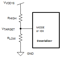
GUID-769CB834-24D4-435E-B89E-A5C9BEA5F906-low.gifFigure 5-2 Strap Pin Connection Diagram
Table 5-2 Strap Configuration Mode Select
MODE NO.VTARGET VOLTAGE RANGEVTARGET STRAP VOLTAGESUGGESTED STRAP RESISTORS (1% TOL)COAX/STPRX MODE
VMINVTYPVMAX(V); V(VDD18) = 1.8 VRHIGH (kΩ )RLOW (kΩ )
0RESERVED
10.179 × V(VDD18)0.213 × V(VDD18)0.247 × V(VDD18)0.37488.723.2STPRAW12 LF
20.296 × V(VDD18)0.330 × V(VDD18)0.362 × V(VDD18)0.5827535.7STPRAW12 HF
30.412 × V(VDD18)0.443 × V(VDD18)0.474 × V(VDD18)0.79271.556.2STPRAW10
4RESERVED
50.642 × V(VDD18)0.673 × V(VDD18)0.704 × V(VDD18)1.20239.278.7COAXRAW12 LF
60.761 × V(VDD18)0.792 × V(VDD18)0.823 × V(VDD18)1.4225.595.3COAXRAW12 HF
70.876 × V(VDD18)V(VDD18)V(VDD18)1.810OPENCOAXRAW10

The strapped values can be viewed and/or modified in the following locations:

  • Coax – Port configuration COAX_MODE (Register 0x6D[2])
  • RX mode – Port configuration FPD3_MODE (Register 0x6D[1:0])