SNLS507C September 2016 – December 2022 DS90UB934-Q1
PRODUCTION DATA
- Features
- 1Applications
- 2Description
- 3Revision History
- Pin Configuration and Functions
- 4Specifications
-
5Detailed Description
- 5.1 Overview
- 5.2 Functional Block Diagram
- 5.3 Feature Description
- 5.4 Device Functional Modes
- 5.5 Programming
- 5.6 Register Maps
- 6Application and Implementation
- Mechanical, Packaging, and Orderable Information
- 7Device and Documentation Support
- Mechanical, Packaging, and Orderable Information
4.7 Recommended Timing for the Serial Control Bus
Over I2C supply and temperature ranges unless otherwise specified.
| MIN | MAX | UNIT | |||
|---|---|---|---|---|---|
| I2C SERIAL CONTROL BUS (Figure 4-4) | |||||
| fSCL | SCL Clock Frequency | Standard-mode | >0 | 100 | kHz |
| Fast-mode | >0 | 400 | |||
| Fast-mode Plus | >0 | 1000 | |||
| tLOW | SCL Low Period | Standard-mode | 4.7 | µs | |
| Fast-mode | 1.3 | ||||
| Fast-mode Plus | 0.5 | ||||
| tHIGH | SCL High Period | Standard-mode | 4 | µs | |
| Fast-mode | 0.6 | ||||
| Fast-mode Plus | 0.26 | ||||
| tHD;STA | Hold time for a start or a repeated start condition | Standard-mode | 4 | µs | |
| Fast-mode | 0.6 | ||||
| Fast-mode Plus | 0.26 | ||||
| tSU;STA | Set Up time for a start or a repeated start condition | Standard-mode | 4.7 | µs | |
| Fast-mode | 0.6 | ||||
| Fast-mode Plus | 0.26 | ||||
| tHD;DAT | Data Hold Time | Standard-mode | 0 | µs | |
| Fast-mode | 0 | ||||
| Fast-mode Plus | 0 | ||||
| tSU;DAT | Data Set Up Time | Standard-mode | 250 | ns | |
| Fast-mode | 100 | ||||
| Fast-mode Plus | 50 | ||||
| tSU;STO | Set Up Time for STOP Condition | Standard-mode | 4 | µs | |
| Fast-mode | 0.6 | ||||
| Fast-mode Plus | 0.26 | ||||
| tBUF | Bus Free Time Between STOP and START | Standard-mode | 4.7 | µs | |
| Fast-mode | 1.3 | ||||
| Fast-mode Plus | 0.5 | ||||
| tr | SCL and SDA Rise Time | Standard-mode | 1000 | ns | |
| Fast-mode | 300 | ||||
| Fast-mode Plus | 120 | ||||
| tf | SCL and SDA Fall Time | Standard-mode | 300 | ns | |
| Fast-mode | 300 | ||||
| Fast-mode Plus | 120 | ||||
| Cb | Capacitive Load for Each Bus Line(1) | Standard-mode | 400 | pF | |
| Fast-mode | 400 | ||||
| Fast-mode Plus | 550 | ||||
| tSP | Input Filter(1) | Fast-mode | 50 | ns | |
| Fast-mode Plus | 50 | ||||
(1) Specification is ensured by design and/or characterization and is not tested in production.
 Figure 4-1 LVCMOS Transition Times
 Figure 4-2 FPD-Link III Receiver VID, VIN, VCM
 Figure 4-3 Deserializer Data Lock Time
 Figure 4-4 I2C Serial Control Bus Timing
 Figure 4-5 SSO Test Pattern for Power Consumption
 Figure 4-6 Deserializer Delay
 Figure 4-7 Deserializer Output Setup/Hold Times
 Figure 4-8 Output State (Setup and Hold) Times
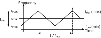
 Figure 4-9 Spread Spectrum Clock Output Profile