SNLS654C April   2021  – November 2024 DP83TC812R-Q1 , DP83TC812S-Q1

PRODUCTION DATA  

  1.   1
  2. Features
  3. Applications
  4. Description
  5. Device Comparison Table
  6. Pin Configuration and Functions
  7. Specifications
    1. 6.1 Absolute Maximum Ratings
    2. 6.2 ESD Ratings
    3. 6.3 Recommended Operating Conditions
    4. 6.4 Thermal Information
    5. 6.5 Electrical Characteristics
    6. 6.6 Timing Requirements
    7. 6.7 Timing Diagrams
    8. 6.8 Typical Characteristics
  8. Detailed Description
    1. 7.1 Overview
    2. 7.2 Functional Block Diagram
    3. 7.3 Feature Description
      1. 7.3.1 Diagnostic Tool Kit
        1. 7.3.1.1 Signal Quality Indicator
        2. 7.3.1.2 Electrostatic Discharge Sensing
        3. 7.3.1.3 Time Domain Reflectometry
        4. 7.3.1.4 Voltage Sensing
        5. 7.3.1.5 BIST and Loopback Modes
          1. 7.3.1.5.1 Data Generator and Checker
          2. 7.3.1.5.2 xMII Loopback
          3. 7.3.1.5.3 PCS Loopback
          4. 7.3.1.5.4 Digital Loopback
          5. 7.3.1.5.5 Analog Loopback
          6. 7.3.1.5.6 Reverse Loopback
      2. 7.3.2 Compliance Test Modes
        1. 7.3.2.1 Test Mode 1
        2. 7.3.2.2 Test Mode 2
        3. 7.3.2.3 Test Mode 4
        4. 7.3.2.4 Test Mode 5
    4. 7.4 Device Functional Modes
      1. 7.4.1  Power Down
      2. 7.4.2  Reset
      3. 7.4.3  Standby
      4. 7.4.4  Normal
      5. 7.4.5  Sleep Ack
      6. 7.4.6  Sleep Request
      7. 7.4.7  Sleep Fail
      8. 7.4.8  Sleep
      9. 7.4.9  Wake-Up
      10. 7.4.10 TC10 System Example
      11. 7.4.11 Media Dependent Interface
        1. 7.4.11.1 100BASE-T1 Master and 100BASE-T1 Slave Configuration
        2. 7.4.11.2 Auto-Polarity Detection and Correction
        3. 7.4.11.3 Jabber Detection
        4. 7.4.11.4 Interleave Detection
      12. 7.4.12 MAC Interfaces
        1. 7.4.12.1 Media Independent Interface
        2. 7.4.12.2 Reduced Media Independent Interface
        3. 7.4.12.3 Reduced Gigabit Media Independent Interface
        4. 7.4.12.4 Serial Gigabit Media Independent Interface
      13. 7.4.13 Serial Management Interface
        1. 7.4.13.1 Direct Register Access
        2. 7.4.13.2 Extended Register Space Access
        3. 7.4.13.3 Write Operation (No Post Increment)
        4. 7.4.13.4 Read Operation (No Post Increment)
        5. 7.4.13.5 Write Operation (Post Increment)
        6. 7.4.13.6 Read Operation (Post Increment)
    5. 7.5 Programming
      1. 7.5.1 Strap Configuration
      2. 7.5.2 LED Configuration
      3. 7.5.3 PHY Address Configuration
    6. 7.6 Register Maps
      1. 7.6.1 Register Access Summary
      2. 7.6.2 DP83TC812 Registers
  9. Application and Implementation
    1. 8.1 Application Information Disclaimer
    2. 8.2 Application Information
    3. 8.3 Typical Applications
      1. 8.3.1 Design Requirements
        1. 8.3.1.1 Physical Medium Attachment
          1. 8.3.1.1.1 Common-Mode Choke Recommendations
      2. 8.3.2 Detailed Design Procedure
      3. 8.3.3 Application Curves
    4. 8.4 Power Supply Recommendations
    5. 8.5 Layout
      1. 8.5.1 Layout Guidelines
        1. 8.5.1.1 Signal Traces
        2. 8.5.1.2 Return Path
        3. 8.5.1.3 Metal Pour
        4. 8.5.1.4 PCB Layer Stacking
      2. 8.5.2 Layout Example
  10. Device and Documentation Support
    1. 9.1 Receiving Notification of Documentation Updates
    2. 9.2 Support Resources
    3. 9.3 Community Resources
    4. 9.4 Trademarks
    5. 9.5 Electrostatic Discharge Caution
    6. 9.6 Glossary
  11. 10Revision History
  12. 11Mechanical, Packaging, and Orderable Information

Signal Traces

PCB traces are lossy and long traces can degrade signal quality. Traces must be kept short as possible. Unless mentioned otherwise, all signal traces must be 50Ω, single-ended impedance. Differential traces must be 50Ω single-ended and 100Ω differential. Make sure impedance is controlled throughout. Impedance discontinuities cause reflections leading to emissions and signal integrity issues. Stubs must be avoided on all signal traces, especially differential signal pairs.
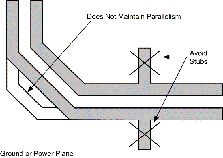
DP83TC812S-Q1 DP83TC812R-Q1 Differential Signal Trace RoutingFigure 8-10 Differential Signal Trace Routing

Within the differential pairs, trace lengths must be run parallel to each other and matched in length. Matched lengths minimize delay differences, avoiding an increase in common mode noise and emissions. Length matching is also important for MAC interface connections. All transmit signal traces must be length matched to each other and all receive signal traces must be length matched to each other. For SGMII differential traces, it is recommended to keep the skew mismatch below 20ps.

Ideally, there must be no crossover on signal path traces. High speed signal traces must be routed on internal layers to improved EMC performance. However, vias present impedance discontinuities and must be minimized when possible. Route trace pairs on the same layer. Signals on different layers must not cross each other without at least one return path plane between them. Differential pairs must always have a constant coupling distance between them. For convenience and efficiency, TI recommends routing critical signals first (that is, MDI differential pairs, reference clock, and MAC IF traces).