SNLS696C April 2021 – July 2024 TSER953
PRODUCTION DATA
- 1
- 1 Features
- 2 Applications
- 3 Description
- 4 Pin Configuration and Functions
- 5 Specifications
-
6 Detailed Description
- 6.1 Overview
- 6.2 Functional Block Diagram
- 6.3
Feature Description
- 6.3.1 CSI-2 Receiver
- 6.3.2 V3Link Forward Channel Transmitter
- 6.3.3 V3Link Back Channel Receiver
- 6.3.4 Serializer Status and Monitoring
- 6.3.5 FrameSync Operation
- 6.3.6 GPIO Support
- 6.4 Device Functional Modes
- 6.5 Programming
- 6.6 Pattern Generation
- 6.7
Register Maps
- 6.7.1
Main Registers
- 6.7.1.1 I2C Device ID Register
- 6.7.1.2 Reset
- 6.7.1.3 General Configuration
- 6.7.1.4 Forward Channel Mode Selection
- 6.7.1.5 BC_MODE_SELECT
- 6.7.1.6 PLL Clock Control
- 6.7.1.7 Clock Output Control 0
- 6.7.1.8 Clock Output Control 1
- 6.7.1.9 Back Channel Watchdog Control
- 6.7.1.10 I2C Control 1
- 6.7.1.11 I2C Control 2
- 6.7.1.12 SCL High Time
- 6.7.1.13 SCL Low Time
- 6.7.1.14 Local GPIO DATA
- 6.7.1.15 GPIO Input Control
- 6.7.1.16 DVP_CFG
- 6.7.1.17 DVP_DT
- 6.7.1.18 Force BIST Error
- 6.7.1.19 Remote BIST Control
- 6.7.1.20 Sensor Voltage Gain
- 6.7.1.21 Sensor Control 0
- 6.7.1.22 Sensor Control 1
- 6.7.1.23 Voltage Sensor 0 Thresholds
- 6.7.1.24 Voltage Sensor 1 Thresholds
- 6.7.1.25 Temperature Sensor Thresholds
- 6.7.1.26 CSI-2 Alarm Enable
- 6.7.1.27 Alarm Sense Enable
- 6.7.1.28 Back Channel Alarm Enable
- 6.7.1.29 CSI-2 Polarity Select
- 6.7.1.30 CSI-2 LP Mode Polarity
- 6.7.1.31 CSI-2 High-Speed RX Enable
- 6.7.1.32 CSI-2 Low Power Enable
- 6.7.1.33 CSI-2 Termination Enable
- 6.7.1.34 CSI-2 Packet Header Control
- 6.7.1.35 Back Channel Configuration
- 6.7.1.36 Datapath Control 1
- 6.7.1.37 Remote Partner Capabilities 1
- 6.7.1.38 Partner Deserializer ID
- 6.7.1.39 Target 0 ID
- 6.7.1.40 Target 1 ID
- 6.7.1.41 Target 2 ID
- 6.7.1.42 Target 3 ID
- 6.7.1.43 Target 4 ID
- 6.7.1.44 Target 5 ID
- 6.7.1.45 Target 6 ID
- 6.7.1.46 Target 7 ID
- 6.7.1.47 Target 0 Alias
- 6.7.1.48 Target 1 Alias
- 6.7.1.49 Target 2 Alias
- 6.7.1.50 Target 3 Alias
- 6.7.1.51 Target 4 Alias
- 6.7.1.52 Target 5 Alias
- 6.7.1.53 Target 6 Alias
- 6.7.1.54 Target 7 Alias
- 6.7.1.55 Back Channel Control
- 6.7.1.56 Revision ID
- 6.7.1.57 Device Status
- 6.7.1.58 General Status
- 6.7.1.59 GPIO Pin Status
- 6.7.1.60 BIST Error Count
- 6.7.1.61 CRC Error Count 1
- 6.7.1.62 CRC Error Count 2
- 6.7.1.63 Sensor Status
- 6.7.1.64 Sensor V0
- 6.7.1.65 Sensor V1
- 6.7.1.66 Sensor T
- 6.7.1.67 CSI-2 Error Count
- 6.7.1.68 CSI-2 Error Status
- 6.7.1.69 CSI-2 Errors Data Lanes 0 and 1
- 6.7.1.70 CSI-2 Errors Data Lanes 2 and 3
- 6.7.1.71 CSI-2 Errors Clock Lane
- 6.7.1.72 CSI-2 Packet Header Data
- 6.7.1.73 Packet Header Word Count 0
- 6.7.1.74 Packet Header Word Count 1
- 6.7.1.75 CSI-2 ECC
- 6.7.1.76 IND_ACC_CTL
- 6.7.1.77 IND_ACC_ADDR
- 6.7.1.78 IND_ACC_DATA
- 6.7.1.79 V3LINK_TX_ID0
- 6.7.1.80 V3LINK_TX_ID1
- 6.7.1.81 V3LINK_TX_ID2
- 6.7.1.82 V3LINK_TX_ID3
- 6.7.1.83 V3LINK_TX_ID4
- 6.7.1.84 V3LINK_TX_ID5
- 6.7.2 Indirect Access Registers
- 6.7.1
Main Registers
- 7 Application and Implementation
- 8 Device and Documentation Support
- 9 Revision History
- 10Mechanical, Packaging, and Orderable Information
7.4.2 Layout Examples
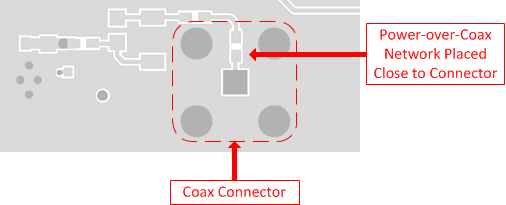
The DS90UB953-Q1 EVM platform can be used to evaluate TSER953. The board layout for the DS90UB953-Q1 EVM is shown in Figure 7-8 and Figure 7-9. All EVM layers are included in DS90UB953-Q1 EVM user's guide (SNLU224).
Routing the V3Link signal traces between the DOUT pins and the connector, as well as connecting the PoC filter to these traces, are the most critical pieces of a successful TSER953 PCB layout. The following list provides essential recommendations for routing the V3Link signal traces between the driver output pins and the FAKRA connector, as well as connecting the PoC filter.
- The routing of the V3Link traces can be all on the top layer or partially embedded in middle layers if EMI is a concern.
- The AC-coupling capacitors must be on the top layer and very close to the receiver input pins to minimize the length of coupled differential trace pair between the pins and the capacitors.
- Route the DOUT+ trace between the AC-coupling capacitor and the FAKRA connector as a 50Ω single-ended micro-strip with tight impedance control (±10%). Calculate the proper width of the trace for a 50Ω impedance based on the PCB stack-up. Make sure that the trace can carry the PoC current for the maximum load presented by the remote sensor module.
- The PoC filter should be connected to the DOUT+ trace through the ferrite bead or an RF inductor. The ferrite bead should be touching the high-speed trace to minimize the stub length seen by the transmission line. Create an anti-pad or a moat under the ferrite bead pad that touches the trace. The anti-pad should be a plane cutout of the ground plane directly underneath the top layer without cutting out the ground reference under the trace. The purpose of the anti-pad is to maintain the impedance as close to 50Ω as possible.
- When routing DOUT+ on inner layers, length matching for single-ended traces does not provide a significant benefit. If the user wants to route the DOUT+ on the top or bottom layer, route the DOUT– trace loosely coupled to the DOUT+ trace for the length similar to the DOUT+ trace length. This may help the differential nature of the receiver to cancel out any common-mode noise that may be present in the environment that may couple on to the signal traces.
 Figure 7-8 TSER953 Serializer DOUT+ Trace Layout
 Figure 7-9 TSER953 Power-over-Coax Layout