SNLU131A February   2013  – June 2024


  1.   1
  2.   Trademarks
  3. 1 DS90UH928QEVM Introduction
    1. 1.1 DS90UH928QEVM Kit Contents
    2. 1.2 System Requirements
    3. 1.3 DS90UH928QEVM Overview
    4. 1.4 Typical Application
  4. 2Quick Start Guide
    1. 2.1 Board Setup
  5. 3Evaluation Hardware Overview
    1. 3.1  Board Overview
    2. 3.2  Power
    3. 3.3  FPD-Link Video Data Output
    4. 3.4  FPD-Link III Interface
    5. 3.5  CML Loop-thru Monitor Interface
    6. 3.6  Controller
    7. 3.7  I2C and Device Addressing
    8. 3.8  I2S and GPIO Interface
    9. 3.9  Device Address, Reset and Mode Selection Inputs
      1. 3.9.1 Output State Select (S1)
      2. 3.9.2 Mode Selection Inputs (S2)
      3. 3.9.3 I2C Address Select (IDx)
      4. 3.9.4 MODE_SEL (S5)
    10. 3.10 Indicators
    11. 3.11 Input/Output Connectors
  6. 4ALP Software
    1. 4.1 Overview
    2. 4.2 Installation
    3. 4.3 Usage
      1. 4.3.1 Information Tab
      2. 4.3.2 Pattern Generator Tab
      3. 4.3.3 Registers Tab
      4. 4.3.4 Scripting Tab
    4. 4.4 Troubleshooting
  7. 5Related Documentation
  8. 6Board Schematic
  9. 7Bill of Materials
  10. 8Board Layout and Layers
  11. 9Revision History

Board Overview

The evaluation board includes circuits and interfaces facilitating the different device features of the DS90UH928Q deserializer, including power, video data, FPD-Link III interface, I2S audio, I2C control, connectors, and configuration switches.
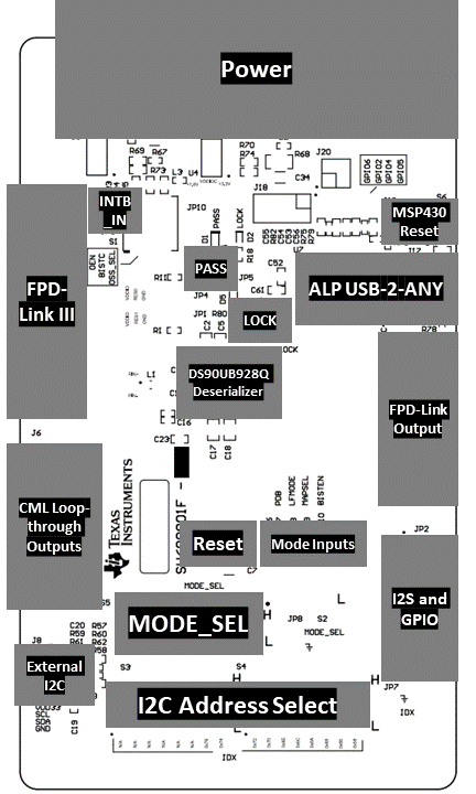
DS90UB928QEVM DS90UB928-Q1EVM Layout Figure 3-1 DS90UB928-Q1EVM Layout