SNLU210C July   2016  – April 2024 DS90UB933-Q1


  1.   1
  2.   Description
  3.   Features
  4.   4
  5. 1Evaluation Module Overview
    1. 1.1 Introduction
    2. 1.2 Kit Contents
  6. 2Hardware
    1. 2.1 Requirements
    2. 2.2 Major Components of DS90UB933-Q1EVM
    3. 2.3 Board Setup Details
      1. 2.3.1 Power Connections
      2. 2.3.2 FPD-Link III Connection
      3. 2.3.3 LVCMOS Input Connector Description (on DS90UB933-Q1 Board)
      4. 2.3.4 Factory Set Switch Settings and Jumpers Default Configuration
        1. 2.3.4.1 Serializer Board Default Configuration
    4. 2.4 Operation with Deserializer
    5. 2.5 Troubleshooting the EVM Setup
  7. 3Software
    1. 3.1 Using I2C
      1. 3.1.1 Default Addresses
      2. 3.1.2 Analog Launch Pad (ALP)
  8. 4Hardware Design Files
    1. 4.1 Schematics
    2. 4.2 PCB Layout
      1. 4.2.1 DS90UB933-Q1EVM Serializer Board Layout
    3. 4.3 DS90UB933-Q1EVM Serializer Board Bill of Materials
  9. 5Additional Information
    1. 5.1 Trademarks
  10. 6Revision History

Serializer Board Default Configuration

GUID-06DACF80-5977-4551-A24E-282F95A1FBB5-low.gif Figure 2-4 Switch S2: Default Settings on Serializer Board
  1. Mode Select Resistor R19 is default set to 4.7kΩ for external oscillator mode. Replace R19 with 100kΩ for PCLK from imager mode.
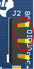
  2. On J2, a 3-pin header is factory placed as shown in Figure 3-4. This selects power from U2 for 1.8V VDDIO and does not have the 3.3V VDDIO option internally.