SNLU224D September 2017 – February 2023 DS90UB953-Q1 , DS90UB953A-Q1
- Trademarks
- 1Introduction
- 2Quick Start Guide
-
3Troubleshooting
- 3.1 Default Addresses
- 3.2 USB2ANY
- 3.3 ALP Software Setup
- 3.4
Troubleshooting ALP Software
- 3.4.1 ALP Loads the Incorrect Profile
- 3.4.2 ALP Does Not Detect the EVM
- 3.4.3 Error When Opening ALP: One Instance of this Application Can Be Active
- 3.4.4 Error Referring to USB2ANY Firmware Update
- 3.4.5 Identifying USB IDs and Corresponding Devices
- 3.4.6 Set up File for Loading Scripts and Create Buttons for Each Script
- 3.5 Additional Troubleshooting – Step-by-Step Guide
- 4Bill of Materials
- 5PCB Schematics
- 6Board Layout
- 7Related Documentation
- 8Revision History
6 Board Layout
The board layout for the DS90UB95x-Q1EVM is shown in #X511 through #X3695.
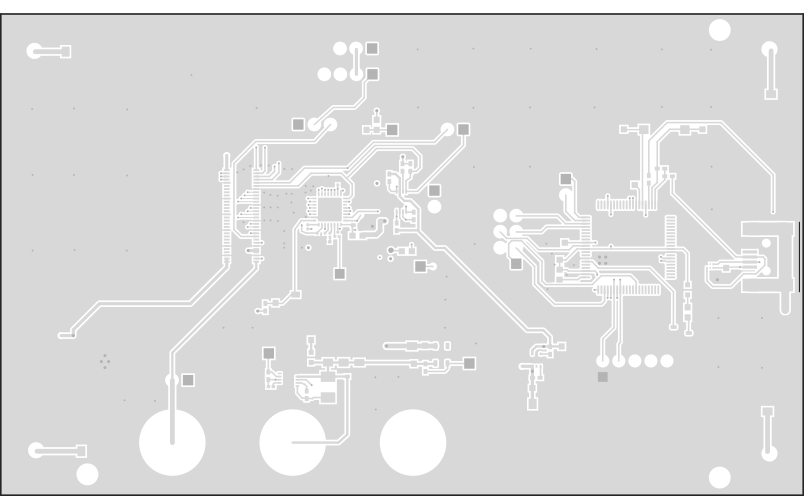 Figure 6-1 Top Layer PCB Layout
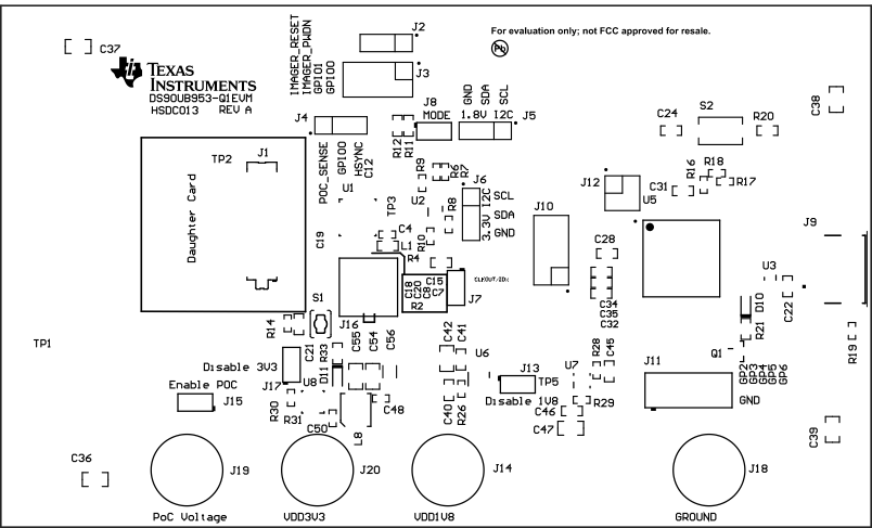 Figure 6-2 Top Overlay
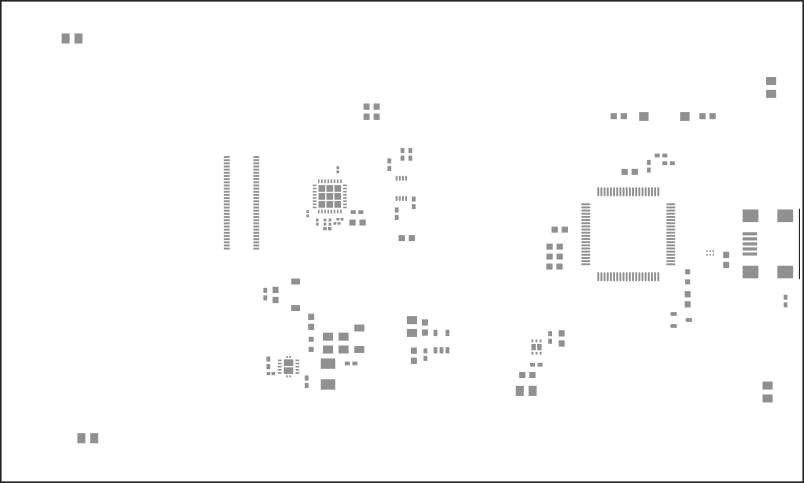 Figure 6-3 Top Paste
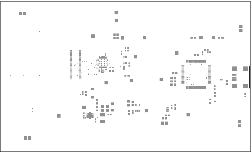 Figure 6-4 Top Solder
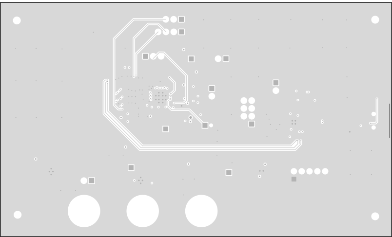 Figure 6-5 Signal Layer 1
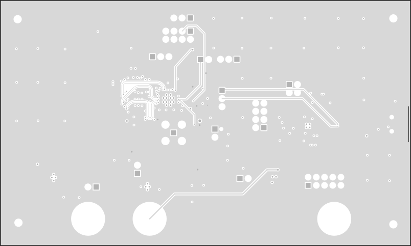 Figure 6-6 Signal Layer 2
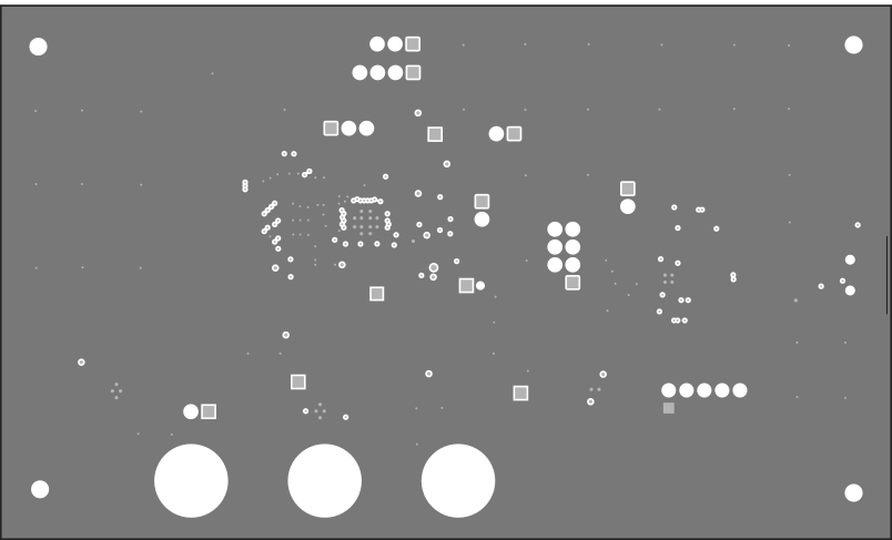 Figure 6-7 Signal Layer 3
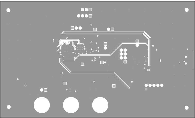 Figure 6-8 Signal Layer 4
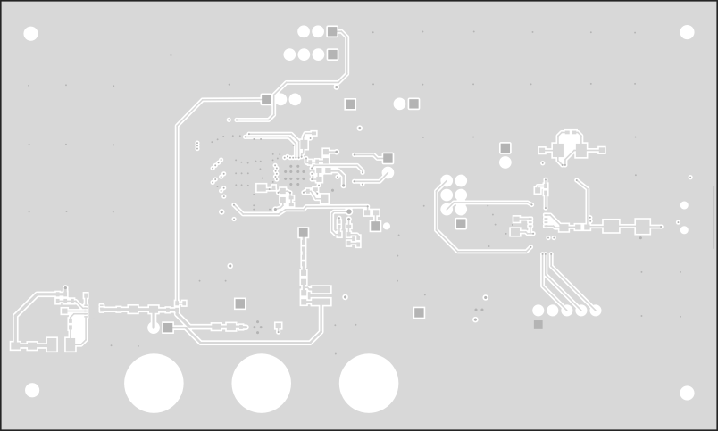 Figure 6-9 Bottom Layer PCB Layout
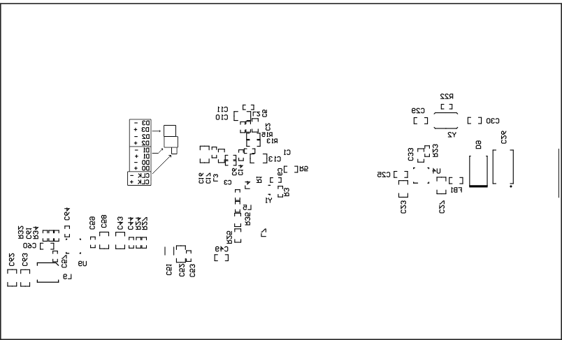 Figure 6-10 Bottom Overlay
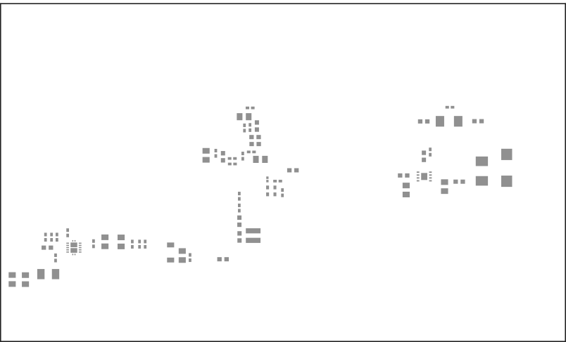 Figure 6-11 Bottom Paste
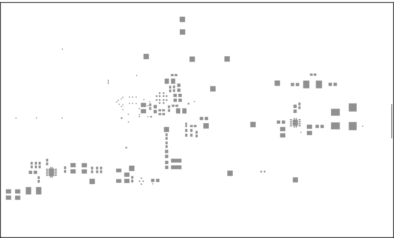 Figure 6-12 Bottom Solder