SNOAA20 January 2019 TLV1805 , TLV1805-Q1
Design Goals
| Supply | Load | Comparator Output Status (OUT) | |
|---|---|---|---|
| Operating Voltage Range | MAX Operating Voltage (VOVER) | SUPPLY < VOVER | SUPPLY ≥ VOVER |
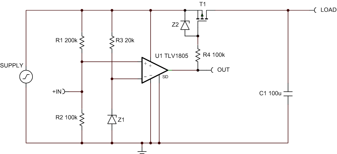
| 12 V to 36 V | 30 V | VOL < 0.4 V | VOH = SUPPLY |
Design Description
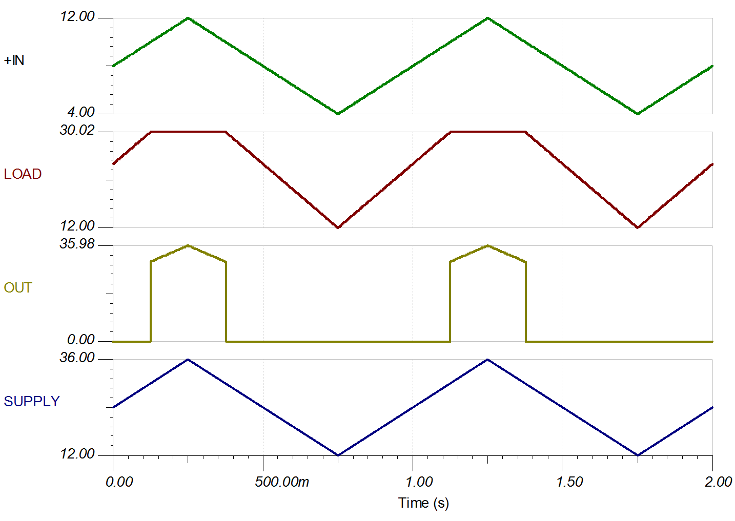
This overvoltage protection circuit uses a high-voltage comparator with a push-pull output stage to control a P-Channel MOSFET that connects the SUPPLY to the LOAD. When the SUPPLY voltage exceeds the overvoltage threshold (VOVER), the output of the comparator goes HIGH and disconnects the LOAD from the SUPPLY by opening the P-Channel MOSFET. Likewise, when the SUPPLY voltage is below VOVER, the output of the comparator is LOW and connects the LOAD to the SUPPLY.
Design Notes
- Select a high-voltage comparator with a push-pull output stage.
- Select a reference voltage that is below the lowest operating voltage range for the SUPPLY.
- Calculate values for the resistor divider so the critical overvoltage level occurs when the input to the comparator (+IN) reaches the comparator's reference voltage.
- Limit the source-gate voltage of the P-Channel MOSFET so that it remains below the device's maximum allowable value.
Design Steps
- Select a high-voltage comparator with a push-pull output stage that can operate at the highest possible SUPPLY voltage. In this application, the highest SUPPLY voltage is 36 V.
- Determine an appropriate reference level for the overvoltage detection circuit. Since the lowest operating voltage for the SUPPLY is 12 V, a 10 V zener diode (Z1) is selected for the reference (VREF).
- Calculate value of R3 by
considering the minimum bias current to keep the Z1 regulating at
10V. A minimum bias current of 100 µA is used along with the minimum SUPPLY
voltage of 12 V.
- Calculate the resistor divider
ratio needed so the input to the comparator (+IN) crosses the reference voltage
(10 V) when the SUPPLY rises to the target overvoltage level (VOVER)
of 30 V.
- Select values for R1 and
R2 that yield the resistor divider ratio of 0.333 V by using the
following equation or using the online at Voltage Divider Calculator.
If using the following equation, choose a value for R2 in the 100 kΩ range and calculate for R1. In this example, a value of 100 k was chosen for R2. - Note that the TLV1805 which is used in application circuit has 15 mV of hysteresis. This means that the actual switching threshold will be 7.5 mV higher than the switching threshold (VREF) when the SUPPLY is rising and 7.5 mV lower when the SUPPLY is falling. The result of the hysteresis is most easily seen in the DC Simulation curve. Since SUPPLY is resistor divided down by a factor of 3, the net impact to the SUPPLY switching threshold is 3 times this amount.
- Verify that the current through the resistor divider is at least 100 times higher than the input bias current of the comparator. The resistors can have high values to minimize power consumption in the circuit without adding significant error to the resistor divider.
- Select a zener diode (Z2) to limit the source-gate voltage (VSG) of the P-Channel MOSFET so that it remains below the device's maximum allowable value. It is common for P-Channel, power MOSFETs to have a VSG max value of 20 V, so a 16 V zener is placed from source to gate.
- Calculate a value for the current
limiting resistor (R4). When SUPPLY rises above 16 V and
Z2 begins to conduct, R4 limits the amount of current
that the comparator output will sink when its output is LOW. With a nominal
SUPPLY voltage of 24 V, the sink current is limited to 80 µA.
Design Simulations
DC Simulation Results
Transient Simulation Results
References:
- Analog Engineer's Circuit Cookbooks
- SPICE Simulation File SNOAA20
- TI Precision Labs
Design Featured Comparator
| TLV1805-Q1 / TLV1805 | |
|---|---|
| VS | 3.3 V to 40 V |
| VinCM | Rail-to-rail |
| VOUT | Push-Pull |
| VOS | 500 µV |
| Hysteresis | 15 mV |
| IQ | 135 µA |
| tPD(HL) | 250 ns |
| TLV1805 | |
Design Alternate Comparator