LMP7704-SP SEE Report
Abstract
This study characterizes the various Single-Event Effects (SEE) of heavy-ion irradiation of the LMP7704-SP. This device is a radiation-hardened, quad-channel, low offset voltage, rail-to-rail input and output (RRIO) precision amplifier with a CMOS input stage. During initial characterization, no incidences of Single-Event Latch-up (SEL) were detected up to LETEFF = 85 MeV-cm2/mg at 125°C. Single-Event Transients (SET) were detected and characterized from LETEFF 2 to 85 MeV-cm2/mg at 25°C.
Subsequent correlation testing identified a subcircuit that is vulnerable to SET, with the potential to cause device burnout under specific circuit criteria. Activation of the ESD clamping cell by a high-energy particle can lead to significant inrush current through the supply pins. Depending on the size, composition, physical distance, and parasitic resistance of the decoupling capacitors, this inrush current can be significant enough to cause localized damage, possibly resulting in a permanent high-conductance path from V+ to V–. The vulnerability can be mitigated by using relatively small (1nF-100nF) C0G decoupling capacitors at the pins, and by isolating larger (>100nF) bulk capacitors from the supply pins with series resistance. Effective shielding, including the intact package body of non-decapped units, was also shown to mitigate the vulnerability. See Extended Characterization for detailed discussion of experiments, root cause, and mitigation techniques.
Trademarks
All trademarks are the property of their respective owners.
1 Overview
The LMP7704-SP is a precision amplifier with low input bias, low offset voltage, 2.5MHz gain bandwidth product, and a wide supply voltage. The device is radiation hardened and operates in the military temperature range of −55°C to +125°C.
The high dc precision of this amplifier, specifically the low offset voltage of ±60µV and ultra-low input bias of ±500fA, make this device an excellent choice for interfacing with precision sensors with high-output impedances. This amplifier can be configured for transducer, bridge, strain gauge, and transimpedance amplification.
| DESCRIPTION | DEVICE INFORMATION |
|---|---|
| TI Part Number | LMP7704-SP |
| MLS Number |
5962-1920601VXC |
| Device Function | Radiation Hardness Assured (RHA), Precision, Low Input Bias, RRIO, Wide Supply Range Amplifiers |
| Technology | VIP050 |
| Exposure Facility | Radiation Effects Facility, Cyclotron Institute, Texas A&M University |
| Heavy Ion Fluence per Run | 1×10⁶ – 1×10⁷ ions/cm2 |
| Irradiation Temperature | 125°C (for SEL testing) |
2 SEE Mechanisms
The primary single-event effect (SEE) events of interest in the LMP7704-SP are single-event latch-up (SEL). From a risk and impact point-of-view, the occurrence of an SEL is potentially the most destructive SEE event and the biggest concern for space applications. The VIP050 process was used for the LMP7704-SP. CMOS circuitry introduces a potential for SEL susceptibility. SEL can occur if excess current injection caused by the passage of an energetic ion is high enough to trigger the formation of a parasitic cross-coupled PNP and NPN bipolar structure (formed between the p-sub and n-well and n+ and p+ contacts). The parasitic bipolar structure initiated by a single-event creates a high-conductance path (inducing a steady-state current that is typically orders-of-magnitude higher than the normal operating current) between power and ground that persists (is latched) until power is removed or until the device is destroyed by the high-current state.
The initial characterization study was performed to evaluate the SEL effects with a bias voltage of 5.5V on VIN and supply voltage of 12V (VS = ±6V). Heavy ions with LETEFF = 85MeV-cm2/mg were used to irradiate the devices. Flux of 105 ions/s-cm2 and fluence of 107 ions/cm2 were used during the exposure at 125°C. The VIP050 process modifications applied for SEL mitigation were shown to be sufficient because the LMP7704-SP exhibited no SEL with heavy-ions up to an LETEFF of 85MeV-cm2/mg at a fluence of 107 ions/cm2 and a chip temperature of 125°C.

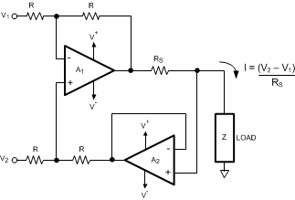
Figure 2-1 Typical LMP7704-SP Application Diagram
Subsequent analysis and retesting of the device identified a vulnerability in the device architecture, with one subcircuit having the potential to cause device burnout under specific circuit criteria. Though the activation of this vulnerability does not give rise to a parasitic bipolar structure, an unintended high-conductance path between V+ and V– still results. If enough current flows along this path, the resulting electrical overstress and associated localized heating can destroy the device. Because the structure can only be activated by a high-energy particle, the scenario is classified as a SEL. See Section 7 for detailed discussion of this vulnerability, including root cause.