SNOAA89 December 2022 AM2431 , AM2432 , AM2434
1 Introduction
FSI bus topology is often used in multi-axis servo applications.
The key requirement for FSI handler is the Low Latency for the communication cycle. Motor drive applications normally use a 20-kHz cycle time and a maximum of eight axes.
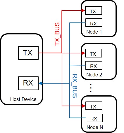
Figure 1-1 shows the FSI bus connection schematic diagram.
 Figure 1-1 FSI Bus Connection Schematic
Diagram
Figure 1-1 FSI Bus Connection Schematic
DiagramIn terms of the amount of data sent and received by the FSI bus, the host device exchanges data with N target nodes in sequence according to the communication cycle. The Sitara AM243x is selected for the host device. For typical applications, the controller node sends 32 bytes and the device nodes reply with 32 bytes in one communication cycle. Considering the maximum of eight axes, the controller node needs to send 8 × 32 bytes through the FSI bus, and receive 8 × 32bytes of response data from the device nodes.
The known design challenges include the following:
- FSI module is not supported by AM243x DMA transfers
- Internal FSI benchmark to transmit 16-bit data (TX 32 bytes + RX 32 bytes) takes about 8.2µs without a data transfer
- Maximum of eight axes can require > 65.6µs to communicate in sequence which does not fulfill the requirements (maximum 50µs, 20 kHz)
Use PRU_ICSSG as the FSI handler (< 5µs with data transfer per axis) for communication to achieve low latency on the FSI data transfer and mapping of FSI data to multiple Arm® cores.
Figure 1-2 shows the communication path and latency estimation.
 Figure 1-2 Communication Path and Latency
Estimation
Figure 1-2 Communication Path and Latency
EstimationTo reduce the overhead of manual data filtering of device nodes, the Frame Tag 4-bits that comes with the FSI bus is used to distinguish eight device nodes. The host device modifies the frame tags in turns in each communication cycle to achieve automatic filtering of the device axis data. Figure 1-3 shows the frame format.
 Figure 1-3 Frame Format of FSI
To realize FSI bandwidth optimization, design a mechanism for FSI data transfer using the ICSSG module with multiple channels as shown in Figure 1-4.
 Figure 1-4 FSI Optimization Using Multiple
Channels and PRU